

Home > Electrical & Electronics > Electrical Control System > Lam Research 810-068158-014 PCBA CIRCUIT BOARD
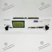
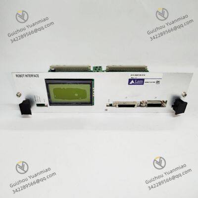
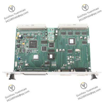
Lam Research 810-068158-014 PCBA CIRCUIT BOARD

Negotiable
MOQ: 1 Piece (Price negotiable depending on order volume and customization)
Key Specifications
Get Latest Price
Material:
Other
Certification:
CE
Function:
Other, Global universal model
Payment & Shipping
Payment Methods:
Port of Shipment:
guizhou
Delivery Detail:
Delivery time depends on order quantity.
Related Products
-
 LAM Research 685-042168-004 VME Bus RackNegotiableMOQ: 1 Piece
 -
Essential LAM 810 - 370141 - 001 PC Safety Interlock PlateNegotiableMOQ: 1 Piece
-
High - Speed LAM 810 - 234640 - 312 Data Communication ModuleNegotiableMOQ: 1 Piece
-
Intelligent LAM 810 - 800081 - 022 System Control BoardNegotiableMOQ: 1 Piece
-
Precision LAM 810 - 801237 - 021 Industrial Control Circuit BoardsNegotiableMOQ: 1 Piece
Material
Other
Certification
CE
Function
Other, Global universal model
Condition
New
Task
Other, Global universal model
Mathematical Model
Other, Global universal model
Signal
Other, Global universal model
Customized
Non-Customized
Structure
Other, Global universal model
I. Basic Information and Core Positioning1. Interpretation of Model and Product Identification

Send Inquiry to This Supplier

* Email
Want the best price?
Post an RFQ now!

1Yr
Business Type
Trading Company
Year Established
2014
Factory Size
1,000-3,000 square meters
Product Certifications
SA8000
You May Also Like
-
High - Quality LAM 810 - 099175 - 012 Industrial Power Interface Board ModuleNegotiableMOQ: 1 Piece
-
Reliable LAM 810 - 099175 - 011 Precision Voltage Input ModuleNegotiableMOQ: 1 Piece
-
Premium LAM 810 - 520659 - 001 Multi - Functional Circuit Board ModuleNegotiableMOQ: 1 Piece
-
Cutting - Edge LAM 810 - 073479 - 215 High - Speed Circuit Board ModuleNegotiableMOQ: 1 Piece
-
High - Precision LAM 810 - 072907 - 005 Industrial PCB Indexer InterfaceNegotiableMOQ: 1 Piece
-
Durable LAM 810 - 072906 - 005 Heavy - Duty Connector BackplaneNegotiableMOQ: 1 Piece
-
Multi - Layer LAM 810 - 069751 - 114 High - Performance Printed Circuit BoardNegotiableMOQ: 1 Piece
-
Compact LAM 810 - 048219 - 015 Efficient Circuit Board ModuleNegotiableMOQ: 1 Piece
-
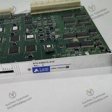
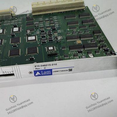
High - Sensitivity LAM 810 - 046015 - 010 Precision Edge Detector Junction BoardNegotiableMOQ: 1 Piece
-
Fast - Speed LAM 605 - 109114 - 004 Industrial Ethernet Card ModuleNegotiableMOQ: 1 Piece


