

2-4inch N/P TYPE Semiconductor Substrate InAs Monocrystalline Crystal Substrates Wafers
Product Spotlights
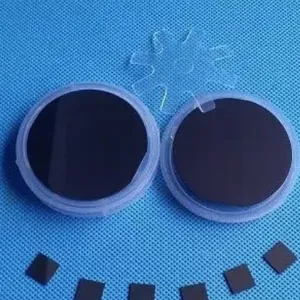
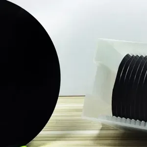
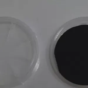
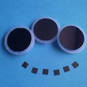
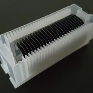
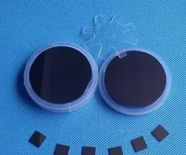
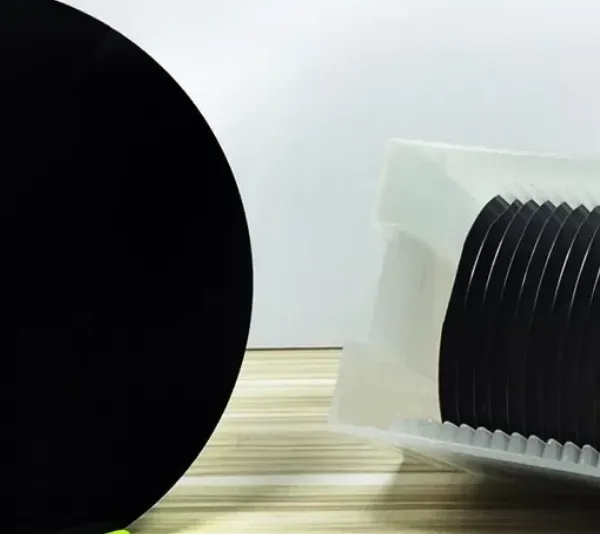
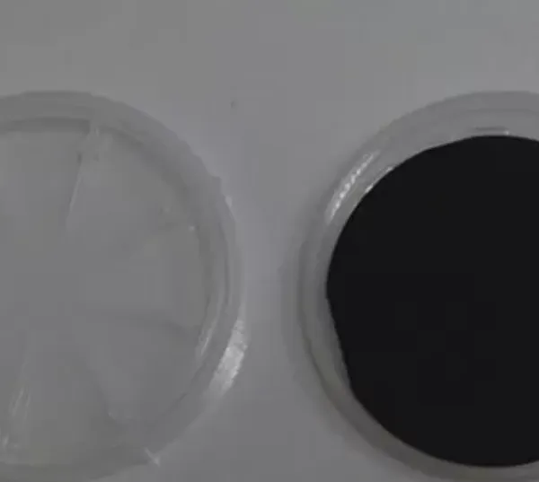
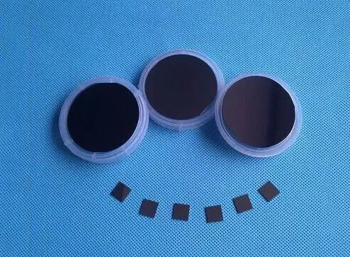
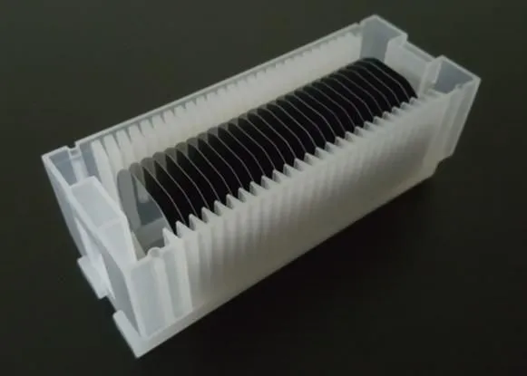
Crystal Substrates Wafers
Related Products
-
 High Purity Sapphire Crystal Watch Face Customized Size Polished SurfaceNegotiableMOQ: 10 Blades
 -
UV&IR Calcium Fluoride (CaF2) WindowsNegotiableMOQ: 10 Blades
-
12 Inch SIC Substrate Silicon Carbide Prime Grade Diameter 300mm Large Size 4H-N Suitable for High Power Device Heat DissipationNegotiableMOQ: 25 Boxes
-
6″ (150mm) High Resistivity Float Zone Silicon WaferNegotiableMOQ: 25 Boxes
-
SOI Wafers Three Layer StructureNegotiableMOQ: 25 Boxes
2-4inch Gallium antimonide GaSb Substrate Single Crystal Monocrystal for Semiconductor
InAsSb/In-AsPSb, InNAsSb and other heterojunction materials can be grown on InAs single crystal as the substrate, and an infrared light-emitting device with a wavelength of 2 to 14 μm can be fabricated. The AlGaSb superlattice structure material can also be epitaxially grown by using InAs single crystal substrate. Mid-infrared quantum cascade laser. These infrared devices have good application prospects in the fields of gas monitoring, low-loss fiber communication, etc. In addition, InAs single crystals have high electron mobility and are ideal materials for making Hall devices.
InAs Monocrystalline Crystal Substrates Wafers Application
InAs single crystal can be used as a substrate material to grow a heterostructure material such as InAsSb/InAsPSb or InAsPSb to fabricate an infrared light-emitting device having a wavelength of 2-12 μm. The InAsPSb superlattice structure material can also be epitaxially grown by using InAs single crystal substrate to fabricate a mid-infrared quantum cascade laser. These infrared devices have good application prospects in the field of gas detection and low loss fiber communication. In addition, InAs single crystals have high electron mobility and are an ideal material for making Hall devices.
InAs Monocrystalline Crystal Substrates Wafers Features
1. The crystal is grown by liquid-sealed straight-drawing technology (LEC), with mature technology and stable electrical performance.
2, using X-ray directional instrument for precise orientation, the crystal orientation deviation is only ±0.5°
3, the wafer is polished by chemical mechanical polishing (CMP) technology, surface roughness 4, to achieve the “open box ready to use” requirements
5, according to user requirements, special specifications product processing
| crystal | dope | type | Ion carrier concentration cm-3 | mobility(cm2/V.s) | MPD(cm-2) | SIZE |
| InAs | un-dope | N | 5*1016 | ³2*104 | Φ2″×0.5mmΦ3″×0.5mm | |
| InAs | Sn | N | (5-20) *1017 | >2000 | Φ2″×0.5mmΦ3″×0.5mm | |
| InAs | Zn | P | (1-20) *1017 | 100-300 | Φ2″×0.5mmΦ3″×0.5mm | |
| InAs | S | N | (1-10)*1017 | >2000 | Φ2″×0.5mmΦ3″×0.5mm | |
| size (mm) | Dia50.8×0.5mm,10×10×0.5mm,10×5×0.5mm can be customized | |||||
| ra | Surface roughness(Ra): | |||||
| polish | single or doubles side polished | |||||
| package | 100 grade cleaning plastic bag in 1000 cleaning room |
—FAQ ––
Q: Are you trading company or manufacturer ?
A: Shanghai Xinkehui New Material Co. Ltd., is a trading company but have a sapphire manufacturer
as a supplier of semiconductor materials wafers for a wide span of applications.
Q: How long is your delivery time?
A: Generally it is 5-10 days if the goods are in stock. or it is 15-20 days if the goods are not in stock,it is according to quantity.
Q: Do you provide samples ? is it free or extra ?
A: Yes, we could offer the sample for free charge but do not pay the cost of freight.
Q: What is your terms of payment ?
A: Payment=1000 USD,
50% T/T in advance ,balance before shipment.

Send Inquiry to This Supplier


You May Also Like
-
Customized Size 8 Inch Sapphire Wafer SubstrateNegotiableMOQ: 25 Blades
-
Synthetic AL2O3 Sapphire Crystal Sapphire Glass Tube and PipeNegotiableMOQ: 10 Pieces
-
12 Inch Sapphire Substrate Dia 300mm C Plane Quartz Wafers BF33NegotiableMOQ: 10 Blades
-
6 Inch N Type Polished Silicon Wafer DSP SiO2 Silicon Oxide WaferNegotiableMOQ: 10 Pieces
-
10*10*0.5 mm Semi P Grade 4H-N Semi SiC Chips Silicon Carbide WaferNegotiableMOQ: 10 Blades
-
200mm 8inch Al2O3 Sapphire Optical Windows , Silicon Substrate SSP DSP 1.0mm C – AxisNegotiableMOQ: 10 Blades
-
12inch C-aixs Al2O3 Sapphire Wafer Double Side PolishedNegotiableMOQ: 10 Blades
-
4Inch Prime Grade 4H-N 1.5mm SIC Silicon Carbide WaferNegotiableMOQ: 10 Blades
-
ZnSe Window Zinc Selenide Optical WaferNegotiableMOQ: 10 Blades
-
ZnTe Crystal Substrate Orientation 110 10x10x0.5mm 10x10x1mmNegotiableMOQ: 10 Blades

