

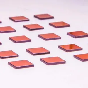
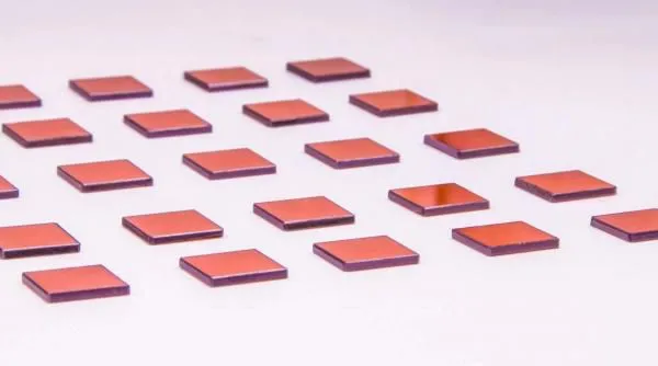
ZnTe Crystal Substrate Orientation 110 10x10x0.5mm 10x10x1mm
Product Spotlights
Related Products
-
 High Purity Sapphire Crystal Watch Face Customized Size Polished SurfaceNegotiableMOQ: 10 Blades
 -
UV&IR Calcium Fluoride (CaF2) WindowsNegotiableMOQ: 10 Blades
-
Customized Size 8 Inch Sapphire Wafer SubstrateNegotiableMOQ: 25 Blades
-
Synthetic AL2O3 Sapphire Crystal Sapphire Glass Tube and PipeNegotiableMOQ: 10 Pieces
-
200mm 8inch Al2O3 Sapphire Optical Windows , Silicon Substrate SSP DSP 1.0mm C – AxisNegotiableMOQ: 10 Blades
ZnTe Crystal Substrate
| Product name | ZnTe crystal substrate |
| Growth Technology | Bridgeman |
| Structure | Cube |
| Lattice constant(A) | 6.103 |
| Density(g/cm3) | 5.633 |
| Melt point(oC) | 1239 |
| Heat Capacity (J/g.k) | 0.16 |
| Coefficient of thermal expansion(10 -6/K) | 8.0 |
| Transparent wavelength(um) | 7-12(>66%) |
| Refractive index | 2.7 |
ZnTe Crystal Substrate
ZnTe crystals are excellent terahertz crystals lt;110> Oriented ZnTe crystals in which THz pulses are detected by free space electro-optical detection.
Terahertz pulses and visible light pulses propagate in a common line through the ZnTe crystal. The terahertz pulse produces birefringence in the ZnTe crystal, which is read out by the linearly polarized visible light pulse. When the visible light pulse and the terahertz pulse are in the crystal at the same time, the visible light polarization will be rotated by the terahertz pulse. Using a l/4 waveplate and beam splitter polarizer and a set of balanced photodiodes, we “map” the THz pulse amplitude by monitoring the rotation of the visible pulse polarization of the ZnTe crystal with respect to the THz pulse after different delay times.
ZnTe Crystal Substrate
ZnTe crystals are II-VI semiconductors with excellent electro-optical properties. they have a sphalerite (ZB) structure under natural conditions, a bandgap width of 2.3ev at room temperature, a large second-order nonlinear coefficient and electro-optical coefficient, and a higher efficiency in radiating and detecting THz electromagnetic waves than other electro-optical crystals, and thus ZnTe crystals are considered to be a better material for THz radiation sources and detectors.ZnTe ZnTe crystals are routinely used as terahertz radiation sources and detectors because the direction of the crystal has the best phase match under laser pulses near 800 nm.
In addition, ZnTe crystals can be widely used in various optoelectronic devices, such as green light-emitting diodes, electro-optical detectors, solar cells and so on.
Product Features:
Applications in THz generation, detection and optical limiters
High crystal purity of 99.995%-99.999
Excellent surface quality

Send Inquiry to This Supplier


You May Also Like
-
12inch C-aixs Al2O3 Sapphire Wafer Double Side PolishedNegotiableMOQ: 10 Blades
-
ZnSe Window Zinc Selenide Optical WaferNegotiableMOQ: 10 Blades
-
2-4inch N/P TYPE Semiconductor Substrate InAs Monocrystalline Crystal Substrates WafersNegotiableMOQ: 10 Blades
-
12 Inch SIC Substrate Silicon Carbide Prime Grade Diameter 300mm Large Size 4H-N Suitable for High Power Device Heat DissipationNegotiableMOQ: 25 Boxes
-
6″ (150mm) High Resistivity Float Zone Silicon WaferNegotiableMOQ: 25 Boxes
-
SOI Wafers Three Layer StructureNegotiableMOQ: 25 Boxes
-
12 Inch Sapphire Substrate Dia 300mm C Plane Quartz Wafers BF33NegotiableMOQ: 10 Blades
-
6 Inch N Type Polished Silicon Wafer DSP SiO2 Silicon Oxide WaferNegotiableMOQ: 10 Pieces
-
10*10*0.5 mm Semi P Grade 4H-N Semi SiC Chips Silicon Carbide WaferNegotiableMOQ: 10 Blades
-
4Inch Prime Grade 4H-N 1.5mm SIC Silicon Carbide WaferNegotiableMOQ: 10 Blades

