

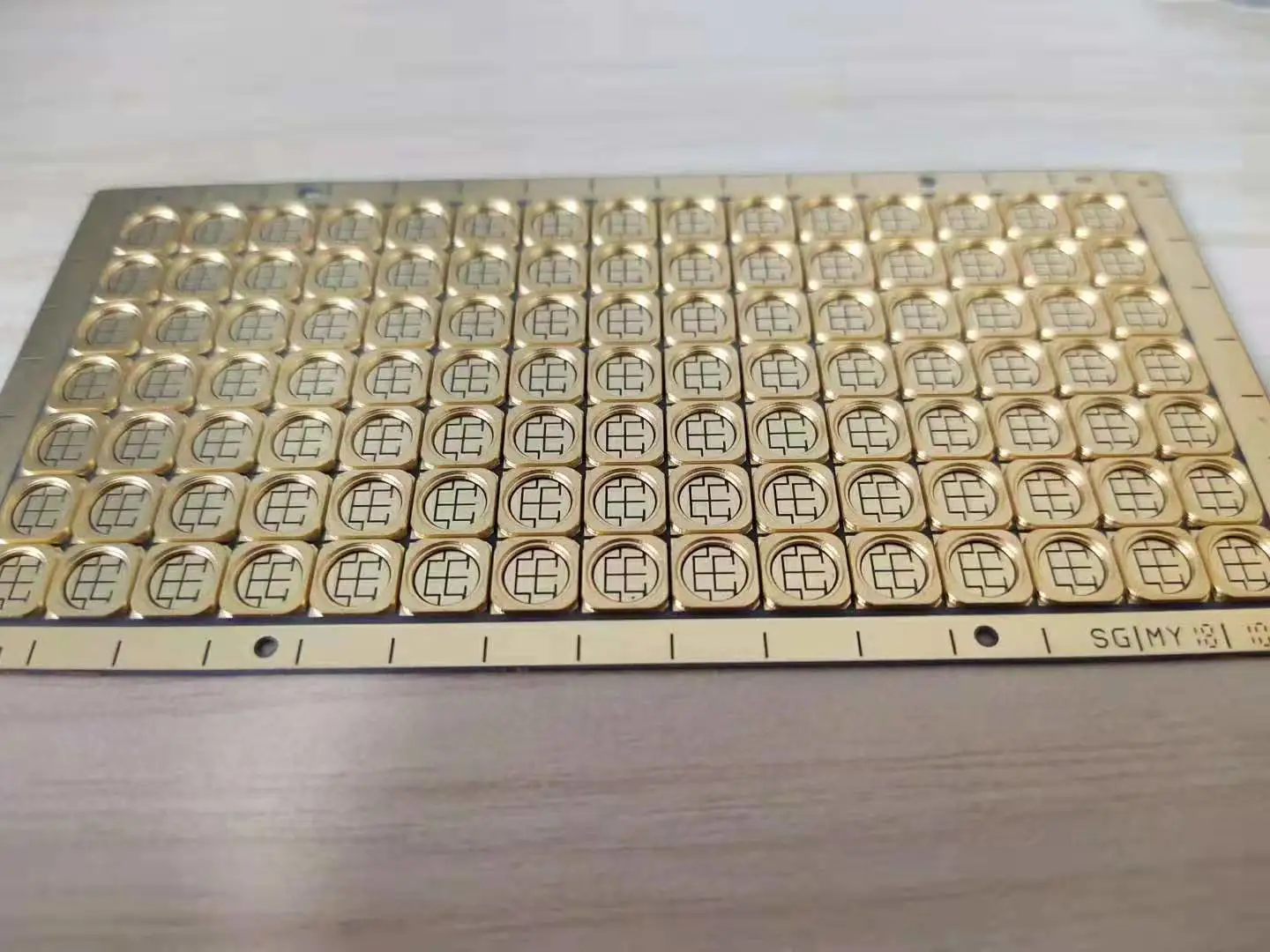
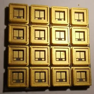
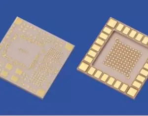
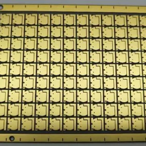
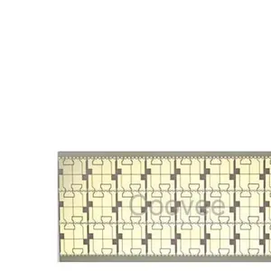
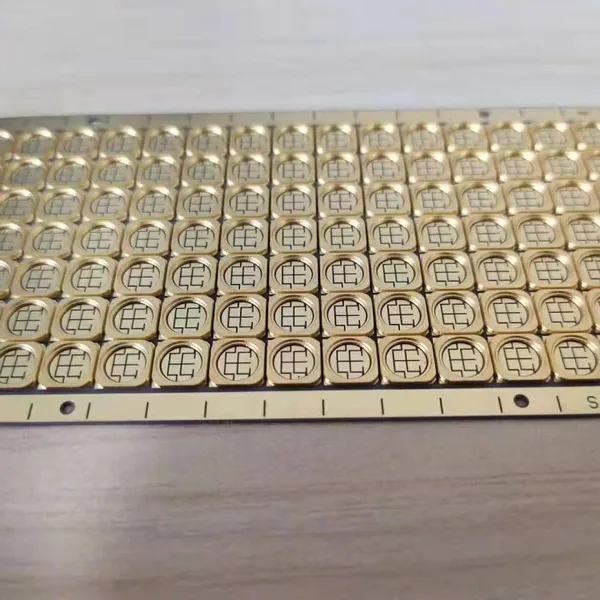
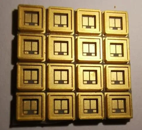
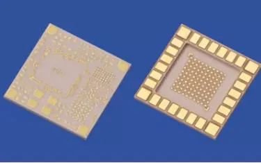
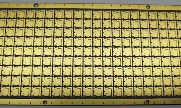
China Chaosheng Electronics' HTCC Alloy Enclosure Gold PCB Gold Plated Ceramic PCB for Dam Enclosure

Product Spotlights
Related Products
-
 2-layer Alumina 96% Ceramic PCB,Double Layer Oxidized 96% Aluminum Ceramic PCBNegotiableMOQ: 500 Units
 -
8LayersHDIPCB,HDI High-frequency High-speed Material PCBNegotiableMOQ: 10 Blades
-
16 Layer Multi-layer Circuit Board PCB,HDI Ultra-thin PCBNegotiableMOQ: 1 Blade
-
16 Layer Multi-layer Circuit Board PCB,HDI Ultra Large PCBNegotiableMOQ: 20 Blades
-
10 Layers, 3rd Order Multi-layer Circuit Board PCB,double-layer Ultra Large PCBNegotiableMOQ: 10 Blades
If you have any needs, please feel free to contact China Chaosheng Electronics Company. Please contact us as follows:
whatsapp:+8613528819118
Skype live: pcb-fpcb88@163.com
E-mail : sales@chaoshengpcb-fpc.com
Contact: Mank. Li
China Chaosheng Electronics' HTCC alloy enclosure gold PCB
* * is a high-end packaging substrate technology that uses HTCC high-temperature co fired ceramics * * as the substrate, Kovar alloy enclosure * * to construct a three-dimensional cavity, and surface * * electroplated gold * * to complete metalization. Its core is used for packaging high reliability, high airtightness, high-power/high-frequency * * devices, and is a core material in the fields of optical communication, semiconductor, aerospace, etc.
1、 Core Definition and Value Positioning
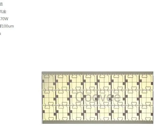
-HTCC substrate: Made of Al ₂ O ∝ or AlN ceramics co fired at 1500-1800 ℃, it combines high thermal conductivity (AlN can reach 170+W/m · K), low thermal expansion (CTE matching chip), high strength, and chemical stability.
-Alloy dam: The mainstream use of Kovar alloy (4J29/Kovar) is matched with the thermal expansion height of ceramic/glass (4.6-5.8 × 10 ⁻⁶/℃), which solves the problems of thermal stress and air leakage, and provides a high rigidity and high gas sealing foundation for the cavity.
-Electroplated Gold Surface: Electroplated gold is applied to the entire surface or key areas (solder pads/dam top surfaces) to achieve low contact resistance, high weldability, corrosion resistance, and high frequency low loss. It is suitable for high-end packaging processes such as gold wire bonding and gold tin eutectic soldering.
-* * Core Value * *: Integrated construction of "ceramic substrate+alloy cavity+gold layer interconnection", meeting * * airtight packaging * * (≤ 10 ⁻⁸ Pa · m ³/s), * * extreme temperature * * (-55 ℃~250 ℃+), * * high-power heat dissipation * * and * * long-term reliability * * requirements.
2、 Key materials and structures
|Module | Typical Materials | Core Function | Key Indicators|
|* * Substrate * * | Al ₂ O ∝/AlN Ceramic | Bearing, Insulation, Heat Dissipation | AlN Thermal Conductivity 170-200 W/m · K; CTE 4.0–7.0×10⁻⁶/℃ |
|Surrounding dam * * | Kovar alloy (4J29) | Chamber forming, thermal expansion matching, airtight sealing | Expansion coefficient synchronized with ceramic/glass; Tensile strength ≥ 500 MPa|
|* * Metalization * * | Gold layer (Au)+nickel barrier layer (Ni) | Low resistance interconnect, solderable, corrosion-resistant, diffusion resistant | Gold purity ≥ 99.99%; Nickel layer 3-5 μ m; Gold layer 0.05-0.2 μ m (solder pad)|
|* * Internal Interconnection * * | W/Mo/Mn Metal Paste | Inter layer 3D Interconnection | Line Width/Spacing 30-50 μ m; Through-hole diameter 50-100 μ m|
3、 Standard process flow
1. Preparation of raw ceramic tape: ceramic powder+binder → ball milling into slurry → casting into shape → drying to obtain raw ceramic tiles.
2. Interlayer processing: Drilling/slotting → screen printing W/Mo metal paste (lines+through holes) → low-temperature drying.
3. Co firing Forming: Multi layer stacking → Hot pressing → High temperature co firing at around 1600 ℃, ceramic densification and metallization are completed simultaneously.
4、 Core technological advantages (compared to traditional PCB)
|Performance Dimension | HTCC Alloy Dam Electrics | Conventional FR-4 PCB | Conventional Ceramic PCB|
|* * Airtightness * * | 10 ⁻⁸ -10 ⁻¹¹ Pa · m ³/s (vacuum/protective gas packaging) | Not available | Same level|
|* * Working temperature * * | -55 ℃~250 ℃+| -40 ℃~130 ℃ | -55 ℃~200 ℃|
|* * Thermal conductivity * * | AlN can reach 170+W/m · K | 0.3-0.8 W/m · K | 20-30 W/m · K|
|* * High frequency performance * * | Low loss, low dielectric, suitable for millimeter wave/optical communication | High loss, significant signal attenuation | Low loss|
|* * Mechanical strength * * | Extremely high, resistant to vibration/impact | General, prone to delamination | High|
|* * Reliability * * | Long lifespan, low failure rate, military/aerospace grade | General | High|
|* * Cost * * | Extremely high (5-10 times FR-4) | Low | Medium|
5、 Typical application scenarios
1. * * Optical communication module * *: VCSEL/laser/detector packaging, with a gold layer to reduce high-frequency losses and a dam to ensure airtight packaging of optical devices.
2. * * Advanced Semiconductor Packaging * *: Power Modules MEMS、 Sensor, 2.5D/3D packaging, ceramic substrate matched with GaN/SiC chip, excellent heat dissipation and thermal stress control.
3. * * Aerospace * *: Satellite communication, radar, aerospace grade sensors, long-term stability and reliability in extreme environments.
4. * * Medical equipment * *: implantable devices, in vitro diagnostic equipment, biocompatible, corrosion-resistant, and highly airtight.
5. * * Industrial high-power * *: Frequency converters, automotive power devices, high-temperature sensors, outstanding high-power heat dissipation and anti vibration capabilities.
6、 Technical difficulties and quality control
-* * Core Challenge * *:
-Co firing shrinkage control (15% -20%) makes it difficult to control dimensional accuracy and warpage.
-The thermal expansion matching and welding interface strength of Kovar dam and HTCC.
-Uniformity, adhesion, and diffusion prevention of the electroplated layer (key to nickel layer).
-Verification of chamber airtightness and long-term reliability.
-* * Key quality control points * *:
-Airtightness: Helium mass spectrometry detection, standard ≤ 10 ⁻⁸ Pa · m ³/s.
-Coating: XRF thickness measurement (gold/nickel thickness ± 0.02 μ m accuracy), adhesion ≥ 0.5 N/mm.
-Size: The height/width error of the dam is ≤ 10 μ m, and the flatness is ≤ 0.05 mm.
-Reliability: Temperature cycling, thermal shock, salt spray, vibration testing, meeting MIL-STD-883 standard.
7、 Difference from LTCC/Sapphire PCB
HTCC alloy dam enclosure electric metal: high-temperature co firing, suitable for high-power/high reliability/airtight packaging, high cost. LTCC: Low temperature co firing (850-900 ℃), suitable for high frequency/miniaturization, with relatively low cost. Sapphire PCB: Single crystal alumina substrate, optically transparent, ultra-high hardness, suitable for optoelectronic/extreme heat dissipation scenarios, with the highest cost. Summary: HTCC alloy dam enclosure electric metal PCB is an integrated solution for high-end packaging. It is based on HTCC, has a deformable dam enclosure cavity, and is interconnected with electric metal, forming an irreplaceable comprehensive advantage in airtightness, heat dissipation, high frequency, and reliability, supporting the core performance and long-term stable operation of cutting-edge electronic devices.

Send Inquiry to This Supplier

You May Also Like
-
28 Layers, 3rd Order Multi-layer Circuit Board PCB,Double Layer Ultra-thin PCBNegotiableMOQ: 1 Blade
-
52 Layers, 3rd Order Multi-layer Circuit Board PCBNegotiableMOQ: 1 Blade
-
12 Layers Multi-layer Circuit Board PCBNegotiableMOQ: 10 Blades
-
12 Layers, 3rd Order Multi-layer Circuit Board PCB,If You Get Rid of the PCBNegotiableMOQ: 10 Blades
-
12 Layers3rd Order Multi-layer Circuit Board PCB, Small BoardNegotiableMOQ: 10 Blades
-
36 Layers, 7th Order Mechanical Blind Buried Hole Multi-layer Circuit Board PCBNegotiableMOQ: 1 Blade
-
China Chaosheng Electronics\' Sapphire Glass-ceramic PCB,PCB,fpcNegotiableMOQ: 1 Blade
-
China Chaosheng Electronics 3D Structured Alumina Ceramic PCB (3D Al ₂ O ∝ PCB) 3D Molding+multi-layer co FiringNegotiableMOQ: 1 Blade
-
Double Layer Transparent FR-4PCB,Multi Layer FR-4 Transparent PCB,Is the Cost of Producing Multi-layer Transparent CircuitNegotiableMOQ: 1 Unit
-
6L Flexible FPC Second OrderNegotiableMOQ: 1 Unit


