








 Contact Platform Support
 Help Center
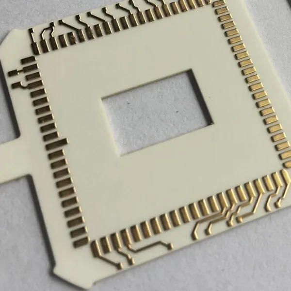
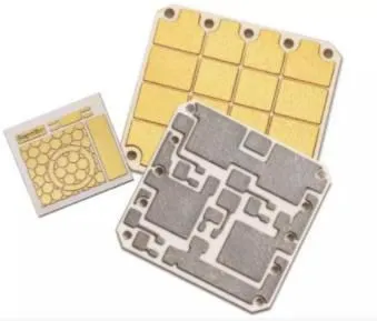
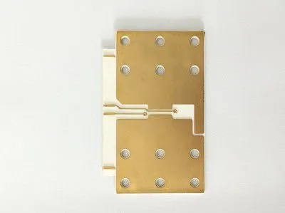
China Chaosheng Electronics' Sapphire Glass-ceramic PCB,PCB,fpc
Product Spotlights


Related Products
-
 China Chaosheng Electronics' HTCC Alloy Enclosure Gold PCB Gold Plated Ceramic PCB for Dam EnclosureNegotiableMOQ: 1 Blade
 -
China Super Sheng, Vibration Motor High Carbon Resistance, Ultra-thin FR-4PCB,High Carbon Resistance PCBNegotiableMOQ: 100 Blades
-
2-layer Alumina 96% Ceramic PCB,Double Layer Oxidized 96% Aluminum Ceramic PCBNegotiableMOQ: 500 Units
-
8LayersHDIPCB,HDI High-frequency High-speed Material PCBNegotiableMOQ: 10 Blades
-
16 Layer Multi-layer Circuit Board PCB,HDI Ultra-thin PCBNegotiableMOQ: 1 Blade
If you have any needs, please contact us:
whatsapp:+8613528819118
Skype live: pcb-fpcb88@163.com
E-mail : sales@chaoshengpcb-fpc.com
Contact: Mank. Li
/
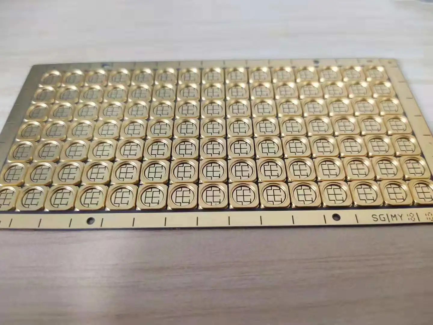
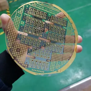
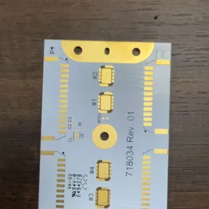
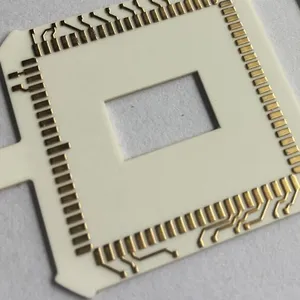
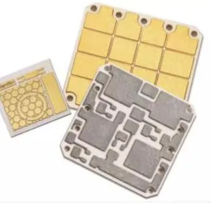
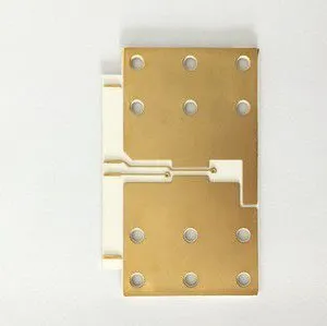
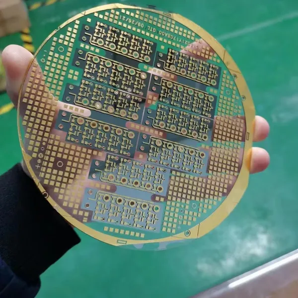
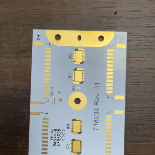
China Chaosheng Electronics' sapphire glass-ceramic PCB (commonly referred to as sapphire PCB) is a specialized circuit board using **monocrystalline alumina (α-Al₂O₃, i.e., sapphire)** as the substrate material, representing a high-end category within the ceramic PCB family. It combines the superior thermal conductivity and insulation properties of ceramics with the exceptional hardness, optical transparency, and chemical inertness of sapphire monocrystals, specifically designed for **high-temperature, high-frequency, high-power, high-reliability, and optoelectronic integration** applications.
1. Core Material Properties
Sapphire is essentially **monocrystalline aluminum oxide**, differing from ordinary polycrystalline alumina ceramic substrates and offering superior performance
- **Ultra High Hardness**: Mohs hardness of 9, second only to diamond, with excellent scratch resistance, wear resistance, and exceptional mechanical strength
- **Extreme Heat Resistance**: With a melting point of **2045°C**, it can withstand temperatures above **300°C** for extended periods, exhibiting exceptional thermal stability
Excellent thermal conductivity: with a thermal conductivity of approximately **40 W/m·K**, far surpassing ordinary glass and FR-4 resin boards
Low thermal expansion: The coefficient of thermal expansion (CTE) is highly compatible with semiconductor chips such as GaN and SiC, minimizing thermal stress
Optical transparency: 190nm~5μm wide spectral transmittance >85%, supporting optical applications from UV to IR
Chemical inertness: Resistant to strong acids and alkalis, moisture-proof, radiation-resistant, and offers excellent insulation properties
II. Core Manufacturing Processes
Sapphire has extremely high hardness and is difficult to process, primarily utilizing **thin/thick film processes** and **laser machining**
1. **Substrate Preparation**: Sapphire crystal rod → Wire cutting → Rough grinding/precision grinding → Chemical mechanical polishing (CMP), achieving atomic-level flatness
2. **Metallization Process (Mainstream)**
- **DPC (Direct Plated Copper)**: Magnetron sputtering for base layer → Electroplating for thickening → Photolithography and etching → Fine circuitry (line width can reach **15μm**)
- **Thin Film Process**: Metalization with films such as Ti/Au, Cr/Au, suitable for ultra-high precision MEMS/optoelectronic products
3. **Key Processes**: **Laser Drilling** (Blind/Through Holes), High-Temperature Annealing, Plasma Cleaning, Surface Gold/Nickel Plating
3. Technical Advantages (Compared to Traditional PCB)
| Performance | Sapphire PCB | Traditional FR-4 PCB | Ordinary Ceramic PCB (Al₂O₃) |
| **Thermal Conductivity** | High (40 W/m·K) | Extremely Low (0.3~0.8) | Medium (20~30) |
| **Operating Temperature** | **-269°C to 300°C+** | -40°C to 130°C | -55°C to 250°C |
| **High-frequency Loss** | **Extremely Low** (dielectric constant 9.8) | High (significant signal attenuation) | Low |
| **Mechanical Strength** | **Extremely High** (Impact/Vibration Resistance) | **Low** (Prone to Delamination) | **Medium** |
3、 Technical advantages (compared to traditional PCB)
table
Performance Sapphire PCB Traditional FR-4 PCB Ordinary Ceramic PCB (Al ₂ O ∝)
High thermal conductivity (40 W/m · K), extremely low (0.3~0.8), medium (20~30)
Operating temperature -269 ℃~300 ℃+-40 ℃~130 ℃ -55 ℃~250 ℃
High frequency loss extremely low (dielectric constant 9.8) high (signal attenuation large) low
Extremely high mechanical strength (impact/vibration resistance), low (easy delamination), and moderate
Optical properties Transparent (UV~IR) Opaque Opaque Opaque
Extremely high reliability (long lifespan, low failure rate), generally high
Extremely high, low, medium cost
4、 Mainstream application areas
Optoelectronics and Semiconductors
LED/GaN devices: heat dissipation substrates for high-power LEDs, laser diodes (LDs), and ultraviolet detectors
Advanced packaging: 2.5D/3D packaging, Chiplet, HBM stacking, solving warpage and thermal management
Optoelectronic Co Packaging (CPO): Utilizing Transparency to Achieve Integrated Photoelectric Thermal Integration
High frequency/5G/millimeter wave
Phased array radar, satellite communication, high-frequency filter: low loss, high stability
High temperature/high power
New energy vehicle power module, aircraft engine control, industrial frequency converter
MEMS and Sensors
Pressure/acceleration sensors, biochips: high precision, high stability, corrosion resistance
Medical/Military Industry
Implantable medical devices, infrared imaging, precision measuring equipment: biocompatible, resistant to extreme environments
5、 Technical Challenges and Trends
main challenges
Extremely high cost: Material, processing, and yield costs are 5-10 times higher than traditional PCBs
Extremely difficult to process: high hardness, high difficulty in drilling, cutting, and metallization, and strict equipment requirements
development trend
Large scale: Breaking through 12 inches, compatible with panel level packaging (PLP)
Composite: Composite with glass, silicon, and diamond, balancing performance and cost
Process Innovation: Laser Direct Writing and Atomic Layer Deposition (ALD) Further Improve Circuit Accuracy

Send Inquiry to This Supplier


You May Also Like
-
16 Layer Multi-layer Circuit Board PCB,HDI Ultra Large PCBNegotiableMOQ: 20 Blades
-
10 Layers, 3rd Order Multi-layer Circuit Board PCB,double-layer Ultra Large PCBNegotiableMOQ: 10 Blades
-
28 Layers, 3rd Order Multi-layer Circuit Board PCB,Double Layer Ultra-thin PCBNegotiableMOQ: 1 Blade
-
52 Layers, 3rd Order Multi-layer Circuit Board PCBNegotiableMOQ: 1 Blade
-
12 Layers Multi-layer Circuit Board PCBNegotiableMOQ: 10 Blades
-
12 Layers, 3rd Order Multi-layer Circuit Board PCB,If You Get Rid of the PCBNegotiableMOQ: 10 Blades
-
12 Layers3rd Order Multi-layer Circuit Board PCB, Small BoardNegotiableMOQ: 10 Blades
-
36 Layers, 7th Order Mechanical Blind Buried Hole Multi-layer Circuit Board PCBNegotiableMOQ: 1 Blade
-
China Chaosheng Electronics 3D Structured Alumina Ceramic PCB (3D Al ₂ O ∝ PCB) 3D Molding+multi-layer co FiringNegotiableMOQ: 1 Blade
-
China Chaosheng Electronics, Fake Double-layer Perforated Flexible FPC, Model CSFPC23650, Ultra-thin, FlexibleNegotiableMOQ: 1 Blade


