








 Contact Platform Support
 Help Center
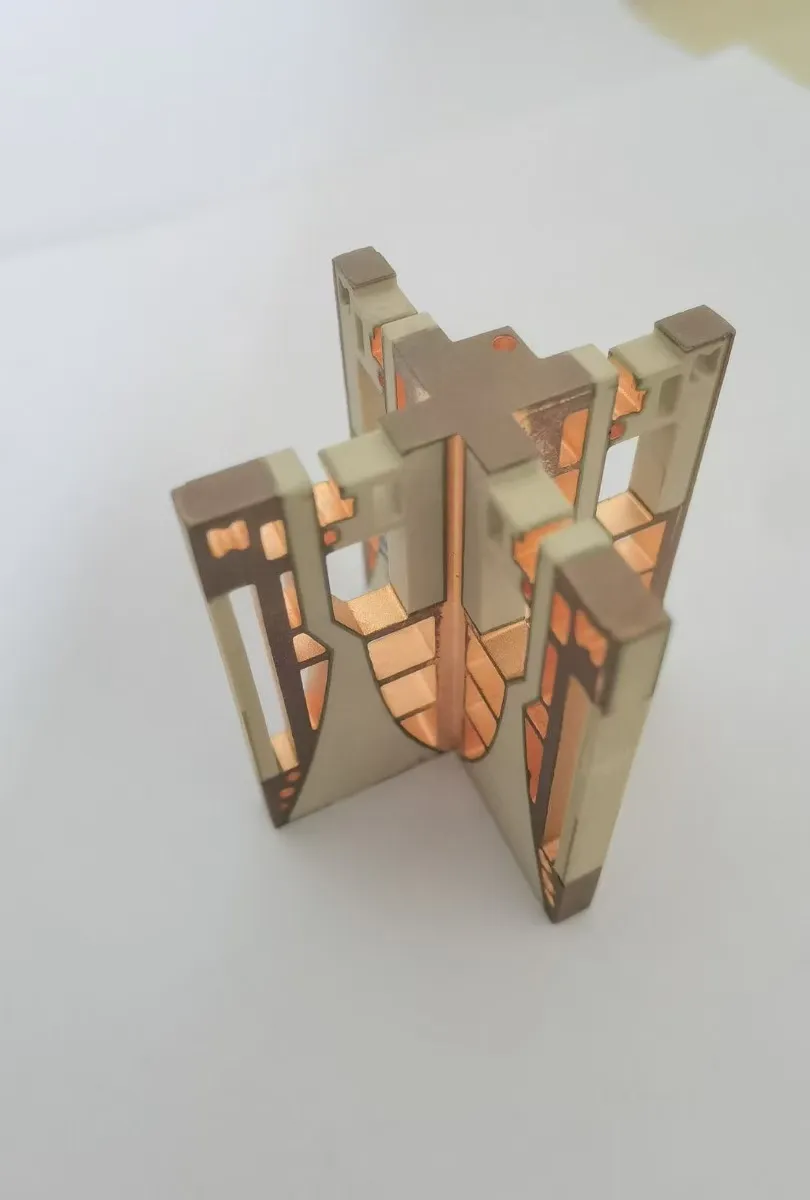
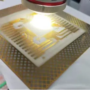
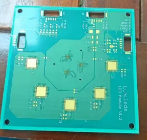
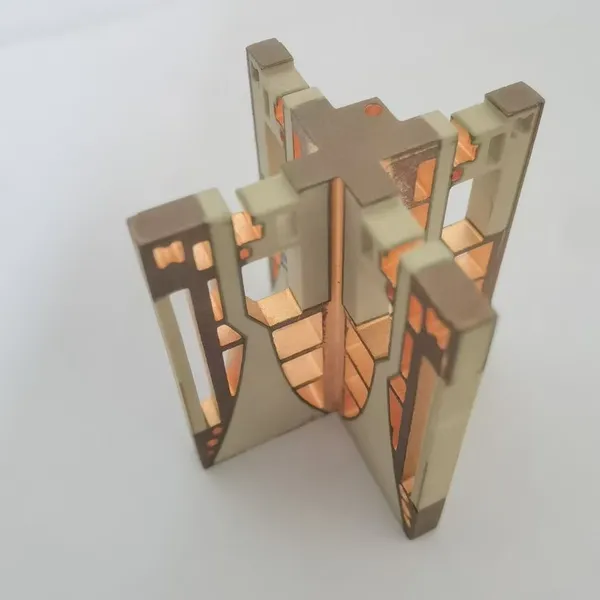
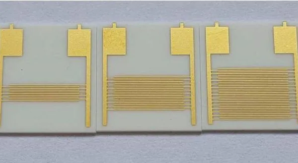
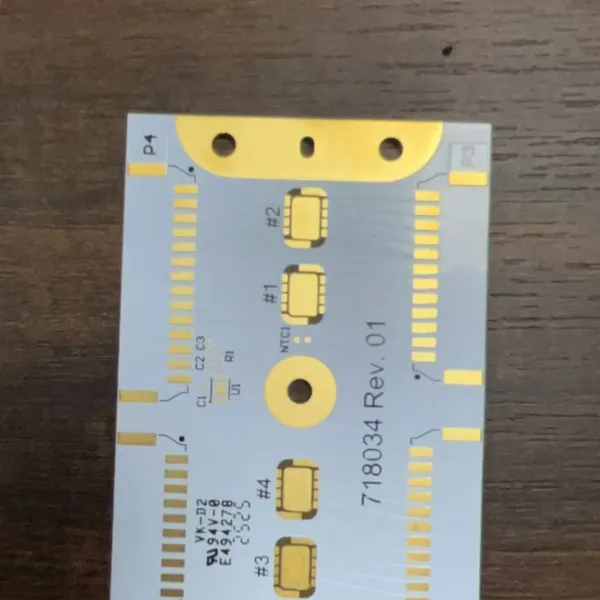
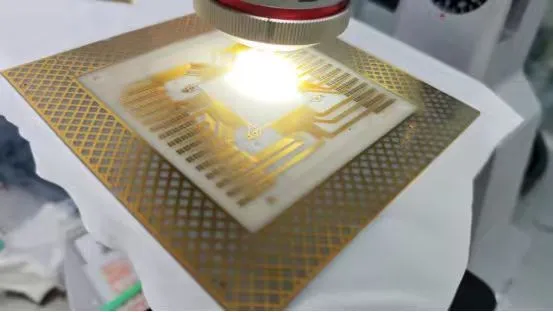
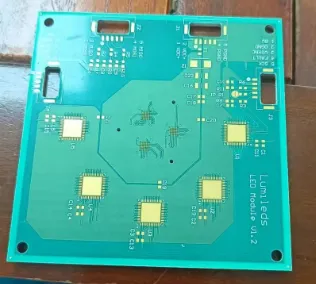
China Chaosheng Electronics 3D Structured Alumina Ceramic PCB (3D Al ₂ O ∝ PCB) 3D Molding+multi-layer co Firing
Product Spotlights


Related Products
-
 2-layer Aluminum Nitride Ceramic PCB,Single Layer Alumina 96% Ceramic PCB,NegotiableMOQ: 500 Units
 -
1 Layer of 96% Alumina Ceramic PCB ,96% Aluminum Nitride Step Ceramic PCBNegotiableMOQ: 20000 Units
-
2-layer Monocrystalline Silicon Ceramic PCB,96% Aluminum Nitride Step Ceramic PCBNegotiableMOQ: 1 Blade
-
2 Layer of 96% Alumina Ceramic PCB,Concave Convex Alumina Ceramic PCBNegotiableMOQ: 1 Blade
-
2-layer 96% Aluminum Nitride Ceramic PCB,Concave Convex Alumina Ceramic PCBNegotiableMOQ: 1 Blade
If you have any needs, please feel free to contact China Chaosheng Electronics Company. Please contact us as follows:
whatsapp:+8613528819118
Skype live: pcb-fpcb88@163.com
E-mail : sales@chaoshengpcb-fpc.com
Contact: Mank. Li
3D structured alumina ceramic board (3D Al ₂ O ∝ PCB) technology from China Chaosheng Electronics
3D structured alumina ceramic board (3D Al ₂ O ∝ PCB) technology from China Chaosheng Electronics
**It refers to an integrated 3D ceramic substrate achieved through 3D molding and multi-layer co firing/additive manufacturing. Unlike traditional flat ceramic plates, it can accommodate complex 3D structures such as vertical through holes, blind holes, cavities, enclosures, heat dissipation channels,
and irregular grooves. It is the core technology for high-power, high-density, airtight, and highly reliable electronic packaging.
1、 Definition and Value of Core Technologies
-3D Structure: It is not a single plane, but a combination of multi-layer interconnection, three-dimensional cavity, and irregular structure (such as
steps, protrusions, deep grooves, enclosures, and built-in flow channels).
-Aluminum oxide substrate * *: 95%~99% Al ₂ O3 * *, high insulation, high thermal conductivity (20~30 W/m · K), high temperature resistance (-55 ℃~200 ℃+), low cost, high strength.
-* * Core Value * *: Solve the three-dimensional wiring, heat dissipation, packaging, and airtightness requirements that cannot be achieved by
flat PCBs, and achieve the integration of electronic component embedding, three-dimensional interconnection, efficient heat dissipation, and high airtightness packaging * *.
2、 Mainstream 3D molding technology route (four major processes)
1 * HTCC/LTCC multi-layer laminated co firing (industrial mainstream)**
**Technical principle: Cast ceramic tiles → Punching/slotting → Printed conductors → Stacking → High temperature co firing → Integrated 3D
structure. Process flow**
1. * * Preparation of raw porcelain * *: Al ₂ O3 powder+binder → Cast into * * 0.1~1mm * * thin strip (raw porcelain).
2. * * 3D structural processing (raw ceramic state)**
-* * Punching * *: Laser/mechanical punching * * vertical through-hole/blind hole * * (diameter 50~200 μ m).
-* * Etching/hollowing out * *: milling grooves, digging cavities, and making steps/enclosures for raw porcelain tiles.
Pre embedded * *: Built in sacrificial core material (such as PVB), sintered to form hollow channels/cavities * *.
3. * * Metalization * *: Screen printing * * W/Mo (HTCC)/Ag Pd (LTCC) * * Line and through-hole filling.
4. * * Stacking and co firing * *: Multi layer precise alignment → Hot pressing → * * 1500~1650 ℃ (HTCC)/850~900 ℃ (LTCC) * * co firing.
5. * * Post processing * *: laser fine-tuning, surface metallization (Ni/Au), cutting, welding.
-* * Core advantages**
-* * Mature mass production * *: high yield, controllable cost, suitable for large quantities.
-* * Diverse structures * *: * * 2-30 layers * *, vertically interconnected, cavities, enclosures, steps.
-* * High airtightness * *: Ceramic integrated sintering, airtightness * * ≤ 10 ⁻⁸ Pa · m ³/s * *.
-* * Disadvantages**
6、 Technology Trends
1. * * Co firing+3D printing fusion * *: Partial 3D printing * * based on casting, balancing mass production and complex structures.
2. * * Ultra low shrinkage * *: * *
3. * * Large scale * *: * * 12 inches+* * 3D ceramic board.
4. * * Multi functional integration * *: * * Integrated heat dissipation+conductivity+insulation+sealing+optics * *.
summary
**3D structured alumina ceramic board * * is used for high-end electronic packaging
**Stereoscopic solution * *.
**HTCC stack burning is the mainstream of industrial mass production, and 3D printing breaks through design limits,
**Injection * * focuses on precision small parts, * * machine welding * * adapts to special scenarios. The core revolves around a three-dimensional structure, high precision, high airtightness, and high reliability, supporting cutting-edge fields such as 5G, optical communication, power semiconductors, and aerospace.
4、 Core technological advantages (compared to traditional PCB)
|Performance Dimension | HTCC Alloy Dam Electrics | Conventional FR-4 PCB | Conventional Ceramic PCB|
|* * Airtightness * * | 10 ⁻⁸ -10 ⁻¹¹ Pa · m ³/s (vacuum/protective gas packaging) | Not available | Same level|
|* * Working temperature * * | -55 ℃~250 ℃+| -40 ℃~130 ℃ | -55 ℃~200 ℃|
|* * Thermal conductivity * * | AlN can reach 170+W/m · K | 0.3-0.8 W/m · K | 20-30 W/m · K|
|* * High frequency performance * * | Low loss, low dielectric, suitable for millimeter wave/optical communication | High loss, significant signal attenuation | Low loss|
|* * Mechanical strength * * | Extremely high, resistant to vibration/impact | General, prone to delamination | High|
|* * Reliability * * | Long lifespan, low failure rate, military/aerospace grade | General | High|
|* * Cost * * | Extremely high (5-10 times FR-4) | Low | Medium|
5、 Typical application scenarios
1. * * Optical communication module * *: VCSEL/laser/detector packaging, with a gold layer to reduce high-frequency losses and a dam to ensure airtight packaging of optical devices.
2. * * Advanced Semiconductor Packaging * *: Power Modules MEMS、 Sensor, 2.5D/3D packaging, ceramic substrate matched with GaN/SiC chip, excellent heat dissipation and thermal stress control.
3. * * Aerospace * *: Satellite communication, radar, aerospace grade sensors, long-term stability and reliability in extreme environments.
4. * * Medical equipment * *: implantable devices, in vitro diagnostic equipment, biocompatible, corrosion-resistant, and highly airtight.
5. * * Industrial high-power * *: Frequency converters, automotive power devices, high-temperature sensors, outstanding high-power heat dissipation and anti vibration capabilities.
6、 Technical difficulties and quality control
-* * Core Challenge * *:
-Co firing shrinkage control (15% -20%) makes it difficult to control dimensional accuracy and warpage.
-The thermal expansion matching and welding interface strength of Kovar dam and HTCC.
-Uniformity, adhesion, and diffusion prevention of the electroplated layer (key to nickel layer).
-Verification of chamber airtightness and long-term reliability.
-* * Key quality control points * *:
-Airtightness: Helium mass spectrometry detection, standard ≤ 10 ⁻⁸ Pa · m ³/s.
-Coating: XRF thickness measurement (gold/nickel thickness ± 0.02 μ m accuracy), adhesion ≥ 0.5 N/mm.
-Size: The height/width error of the dam is ≤ 10 μ m, and the flatness is ≤ 0.05 mm.
-Reliability: Temperature cycling, thermal shock, salt spray, vibration testing, meeting MIL-STD-883 standard.

Send Inquiry to This Supplier


You May Also Like
-
2-layer Aluminum Nitride Ceramic PCBNegotiableMOQ: 500 Blades
-
2-layer Aluminum Nitride Ceramic Controlled Deep Step Ceramic PCBNegotiableMOQ: 500 Blades
-
2-layer Aluminum Nitride Ceramic Concave Step Ceramic PCBNegotiableMOQ: 1 Blade
-
2-layer Alumina Ceramic Thick Copper Ceramic PCBNegotiableMOQ: 1 Blade
-
2-layer Aluminum Nitride Ceramic Thick Copper Ceramic PCB+embedded Process Ceramic PCBNegotiableMOQ: 1 Blade
-
Metal Edged Ceramic PCB,Non Trace Metal Edging Ceramic PCBNegotiableMOQ: 1 Blade
-
China Chaosheng Electronics, Fake Double-layer Perforated Flexible FPC, Model CSFPC23650, Ultra-thin, FlexibleNegotiableMOQ: 1 Blade
-
China Super Sheng, Vibration Motor High Carbon Resistance, Ultra-thin FR-4PCB,High Carbon Resistance PCBNegotiableMOQ: 100 Blades
-
China Super Sheng, Ultra Large Size Multi-layer Whole Board Gold-plated Circuit Board PCB, Nuclear Product PCBNegotiableMOQ: 1 Blade
-
China Chaosheng Electronics | 1650 × 700mm Ultra Large Size Four Layer 3OZ Thick Copper Nickel Gold Circuit Board PCBNegotiableMOQ: 1 Blade


