

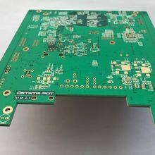
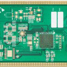
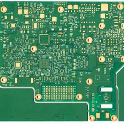
16 Layer Multi-layer Circuit Board PCB,HDI Ultra Large PCB

Product Spotlights
Related Products
-
 10 Layers, 3rd Order Multi-layer Circuit Board PCB,double-layer Ultra Large PCBNegotiableMOQ: 10 Blades
 -
28 Layers, 3rd Order Multi-layer Circuit Board PCB,Double Layer Ultra-thin PCBNegotiableMOQ: 1 Blade
-
52 Layers, 3rd Order Multi-layer Circuit Board PCBNegotiableMOQ: 1 Blade
-
12 Layers Multi-layer Circuit Board PCBNegotiableMOQ: 10 Blades
-
12 Layers, 3rd Order Multi-layer Circuit Board PCB,If You Get Rid of the PCBNegotiableMOQ: 10 Blades
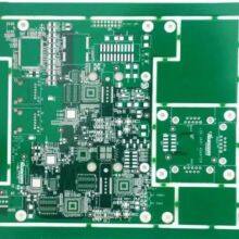
| If you have any needs, please feel free to contact China Chaosheng Electronics Company. Please contact us as follows: whatsapp:+8613528819118 Skype live: pcb-fpcb88@163.com E-mail : sales@chaoshengpcb-fpc.com Contact: Mank. Li Ultra large PCB, single-layer ultra large PCB, double-layer ultra large PCB, multi-layer ultra large PCB, HDI ultra large PCB, Ultra large PCB, single-layer ultra large PCB, double-layer ultra large PCB, multi-layer ultra large PCB, HDI ultra large PCB Product Name: Communication Equipment Product Board: FR-4, TG150 Layers: 16 layer multi-layer circuit board PCB Minimum line width/spacing: 4/4mil Finished product size: 145x125mm/1 * 1pcs Surface technology: Sinking gold, red solder mask Copper thickness: 35um for inner and outer layers Plate thickness: 1.60mm Minimum aperture: 0.25mm, no laser hole/mm, Features: Difficulties such as communication equipment Usage: Engine, electric motor, inductor, orange equipment, etc Process Capability Table | ||||
| Technical ltem | MassProduct | Advanced Technology | ||
| 2015 | 2021 | 2025 | ||
| Max.Layer Count | 80 layer | 100 layer | 100 layer | |
|
PCB through hole board |
2~80 layer | 2~100 layer | 2~100 layer | |
|
Maximum size through hole 1~2 |
37〞*98.50" | 43.3〞*118.11" | 43.3〞*118.11" | |
|
Minimum line width and spacing |
10(0.40) | 10(0.40) | 7.50(0.30mm) | |
| Minimum mechanical hole(mm) |
12(0.50) | 10(0.40) | 8.50(0.35mm) | |
|
Maximum size through hole 4~22 layers |
37〞*43.30" | 43.3〞*43.30" | 43.3〞*43.30" | |
|
Maximum size through hole 4~22 layers |
31.50 ″*59" | 31.50 ″*70.86" | 31.50 ″*70.86" | |
|
Maximum size through hole 4~22 layers |
10(0.40) | 10(0.40) | 7.50(0.30mm) | |
| Minimum line width and spacing for multi-layer large-sized PCBs |
10(0.40) | 10(0.40) | 7.50(0.30mm) | |
|
Maximum size of multi-layer through- hole : 4-22 layers with the smallest hole |
12(0.50) | 10(0.40) | 8.50(0.35mm) | |
| Maximum size HDI 4~36 layers | 31.50 ″*55" | 31.50 ″*55" | 31.50 ″*55" | |
| Minimum line width and line spacing of large size PCB |
Through hole 12 / 12milHDI14 /14mil |
Through hole 10/10 milHDI12 / 12mil |
Through hole 8 / 8milHDI12 / 12mil |
|
| The largest board ruler 1 → the smallest hole of 18 layers |
Through hole 0.50mmHDI :0.45mm |
Through hole 0.50mm HDI : 0.45mm |
Through hole 0.50mmHDI : 0.45mm |
|
| The layer number of FPC | 1~36layer | 1~60layer | 1~60layer | |
| Maximum size of flexible FPC |
19.68〞*55" | 28〞*59" | 31.49〞*118.12" | |
| Maximum size of flexible FPC with soft hard combination |
19.68〞*55" | 28〞*59" | 31.49〞*118.12" | |
|
FPC (roll to roll) maximum size |
19.68 ″*7874" | 19.68 ″*7874" | 19.68 ″*7874" | |
|
Maximum size of FPC single chip shipment |
19.68 ″*118.11" | 19.68 ″*196.8" | 19.68 ″*196.80" | |
| The layer number of FPC | 2~18 layer | 2~36 layer | 2~42 layer | |
|
Maximum size of layered board |
19.68 ″*35" | 19.68 ″*43" | 19.68 ″*43" | |
|
Number of through-hole layers |
2~20layer | 2~30 layer | 2~40 layer | |
|
Hard and soft HDI layers |
2~14 layer | 2~18 layer | 2~22 layer | |
|
Maximum size of soft and hard combination |
19.68 ″*43" | 19.68 ″*49" | 19.68 ″*49" | |
|
FPC/soft-hard combination arbitrary interconnection HDI |
4+X+4Interconnect HDI |
5+X+5Interconnect HDI | 6+X+6Interconnect HDI |
|
|
HDIPCB layers |
4~36layer | 4~60layer | 4~80 layer | |
|
Anylayer HDI PCB |
4+X+4Interconnect HDI |
5+X+5、Interconnect HDI | 8+X+8、Interconnect HDI |
|
|
HDIPCB maximum board size |
24"*52" | 43"*49" | 43"*49" | |
|
Number of through hole layers of high frequency board |
2~18 layer | 2~36 layer | 2~60 layer | |
| HDI layers ofhighfrequency board |
2~16 layer | 2~24 layer | 2~60layer | |
| Maximum size of high frequency board |
37 ″*43" | 43 ″*49" | 43 ″*49" | |
|
Number of ceramic plates |
1-2 layer | 1~4 layer | 1~6 layer | |
|
Ceramic plate thickness |
0.60mm-1.60mm | 0.38mm-20.0mm | 0.38mm-20.0mm | |
|
Maximum size of ceramic plate |
100*150mm | 150*190mm | 150*650mm | |
|
Minimum aperture of ceramic plate |
0.50mm | 0.35mm | 0.35mm | |
|
Minimum line width and line spacing of ceramic board |
16/16mil | 12/12mil | 10/10mil | |
|
Number of layers of metal copper substrate |
1-2 layer | 1~4 layer | 1~6 layer | |
|
Maximum line width and line spacing of metal iron substrate |
12/12mil | 4/4mil | 4/4mil | |
|
Number of layers of metal aluminum substrateHDI |
1-2 layer | 1~4 layer | 1~6 layer | |
|
Maximum size of metal substrate |
37 ″*43" | 25.59 ″*59" | 25.59 ″*59" | |
| The smallest hole of the metal substrate |
0.50mm | 0.35mm | 0.35mm | |
|
Minimum line width and line spacing of metal substrate |
8/8mil | 4/4mil | 4/4mil | |
| Transparent FR- 4 material layers |
1-2layer | 1-2layer | 1-8layer | |
| Transparent FR-4 minimum hole |
0.35mm | 0.35mm | 0.35mm | |
| Transparent FR-4 minimum line width and spacing |
4/4Mil | 4/4Mil | 3.5/3.5Mil | |
| Transparent FR- 4 maximum size |
23.63*47.25″ | 23.63*47.25 ″ | 23.63*47.25 ″ | |
| Number of tempered glass base layers |
1-2layer | 1-2layer | 1-2layer | |
| Minimum line width and spacing of glass |
4/4Mil | 4/4Mil | 3.5/3.5Mil | |
| The smallest hole in glass |
0.35mm | 0.35mm | 0.35mm | |
| Maximum size of glass |
23.63*47.25″ | 23.63*47.25 ″ | 23.63*47.25 ″ | |
| Number of layers of transparent PETmaterial |
1-2layer | 1-2layer | 1-2layer | |
| Maximum size of transparent PET |
19.68 ″*7874" | 19.68 ″*7874" | 19.68 ″*7874" | |
|
The company's main product types |
Halogen free materials, high TG materials, high-frequency materials, high-speed materials, metal materials, glass materials, embedded materials, transparent FR- 4 materials, high thermal conductivity metals, high thermal conductivity aluminum substrates, environmentally friendly circuit boards, BT materials, ABF materials, and other imported materials, DU busbars, iron-based and metal based (core) mixed pressure plates, embedded buried copper, buried resistors, buried capacitors, buried ceramic bead plates, buried ceramics, ceramic mixed pressure plates, multi-layer ceramics, ultra-thin BT plates, ultra-thin PCBs, ultra-thin PCBs, multi-layer aluminum substrates, multi-layer ceramic plates, multi-layer ultra-thin HDI、 High frequency mixed voltage, differential impedance board, thick copper plate, gold-plated plate, high and low copper, high and low copper, high carbon resistance, transparent multilayer, glass plate, HDI arbitrary order (cross blind buried) Anylayer, flexible double-sided, flexible multilayer, soft hard combination HDI, roll to roll FPC, ultra long size, ultra large size board (single, double, multi-layer) PCB production and product design, product development, software development, etc |
|||
| Main material |
Rogers, Taikoni, Yaron, Mitsui, Isola, 3M, Taiyao, Taiguang, Tenghui, Shengyi,Lianmao, Nanya, Doosan, DuPont, Taihong, Hongren, Xinyang, Nippon Steel, Teflon,Yasen, Panasonic, RCC, Mitsui, Mitsubishi, Yingye, 3M, Kyocera, Jiuhao, Zhongci,Huaqing, Aishengda, Sliton, Kaichangde, Tongxin, Beige, Yalong, Taikoni,Hitachi, Laird System, etc |
|||
|
Main material categories |
Halogen-free、halogenated、 high thermal conductivity, high TG135 、TG140、 TG150、 TG170、TG180、TG240、TG320 |
|||
| Build-up Material | FR-4 ,TG150,TG70,TG180 | |||
| Conventional plate thickness (mm) |
Min.1-2L(mm) | 0.10mm | 0.10-12.0mm | 0.10-18.0mm |
| Min.4-10L(mm) | 0.35mm | 0.35mm~10.0mm | 0.35-18.0mm | |
| Min.12L(mm) | 0.43 | 0.38~10.0mm | 0.38~18.0mm | |
| Min.16L(mm) | 0.53 | 0.45~10.0mm | 0.45~18.0mm | |
| Min.18L(mm) | 0.63 | 0.51~10.0mm | 0.51~18.0mm | |
| Min.52L(mm) | 0.8 | 0.65~10.0mm | 0.65~18.0mm | |
| MAX(mm) | 3.5 | 12.0mm | 18.0mm | |
|
Copper plate thickness and copper thickness |
1-2 layerCU | 700um | 875um | 875um |
| Layers 4-20 |
4-12layer | 4-16layer | 4-22layer | |
| Inner layer copper thickness(um) |
875um | 1050um | 1225um | |
|
Outercopperthickness |
210um | 350um | 525um | |
|
Thick copper finished plate thickness |
8.0mm | 12.0mm | 18.0mm | |
| IC substrate |
layerHDI | 1-10layer | 1-14layer | 1-16layer |
| Line width and spacing |
50um | 25um | 15um | |
| copper thickness |
8-10um | 10-12um | 12-15um | |
| Min.CoreThickness um(mil) | 254" (10.0) | 0.15~254(10.0mm) | 0.15~254(10.0mm) | |
| Min.Build up Dielectric |
38(1.5) | 25(1.0) | 25(1.0) | |
|
BaseCopperWeigh t |
Inner Layer | 1/4-8 OZ | 1/4-0.30mm | 1/4-0.30mm |
| Out Layer | 1/4-10 OZ | 1/4-30 OZ | 1/4-30 OZ | |
| Gold thick | 1~40u" | 1~200u" | 1~200u" | |
| Nithick | 76~127u" | 1~250u" | 1~250u" | |
|
Min.HOle/Land um(mil) |
150/300(6/12) | 100/200(4/8) | 100/200(4/8) | |
|
Min.Laser via/landum(mil) |
60/170(2.4/6.8) | 50/150(2/6) | 50/150(2/6) | |
|
Min. IVH、Hole size/landum(mil) |
150/300(6/12) | 100/200(4/8) | 100/200(4/8) | |
| DieletricThickness | 38(1.5) | 32(1.3) | 32(1.3) | |
| 125(5) | 125(5) | 125(5) | ||
| SKipvia | Yes | Yes | Yes | |
| viaoNhie(laserviaon BuriedPTH) | Yes | Yes | Yes | |
| Laser Hole Filling | Yes | Yes | Yes | |
| Technicalltem | MassProduct | Advanced Technology | ||
| Hole depth/diameter | Through Hoie | 25:01 :00 | 35:01 :00 | 40:01 :00 |
| AspctRatio | MicroVia | 0.8 :1 | 0.8 :1 | 0.8 :1 |
| copperFilling Dimple Size | 10(0.40) | 5(0.20) | 5(0.20) | |
|
Minimumouter line width/ spacing |
Inner layer line width and spacing | 38/38(1.5/1.5) | 38/38(1.5/1.5) | 38/38(1.5/1.5) |
|
PlatedLayerum(mil) |
38/38(1.5/1.5) | 38/38(1.5/1.5) | 38/38(1.5/1.5) | |
| BGAPitchmm(mil) | 0.4 | 0.4 | 0.4 | |
| PHMin.Hole rlng um(mil) | 75(3) | 62.50(2.50 | 62.50(2.50 | |
| Line Width control |
±0.50 | ±0.50 | ±0.50 | |
| 2.5mil≤L/W | ±0.50 | ±0.50 | ±0.50 | |
| ≤3mil(mil) | ±0.60 | ±0.60 | ±0.60 | |
| SolderMask Registration um(mil) |
±25 | ±25 | ±25 | |
| Solder masThickness |
Lines Minum(mil) | 10(0.40) | 10(0.40) | 10(0.40) |
| Lines Minum(mil) | 30(1.20) | 30(1.20) | 30(1.20) | |
| CopperMinum(mil) | 10(0.40) | 10(0.40) | 10(0.40) | |
| CopperMax um(mil) |
30(1.20) | 30(1.20) | 30(1.20) | |
| Mln.Solder Mask opening um(mil) |
250(10) | 200(8) | 200(8) | |
|
Structure |
Stacking layer by layer |
5+N+5 | 6+N+6 | 7+N+7 |
| Sequenetlal Bu il-up | 42Any Layer | 46Any Layer | 60Any Layer | |
| Stacking layer by layer |
N+N | N+N | N+N | |
| N+X+N | N+X+N | N+X+N | ||
| Sequenetlal Lamination |
4+(N+X+N)+4 | 5+(N+X+N)+5 | 6+(N+X+N)+6 | |
|
Multi-layer stepped structure |
Multi- layer stacking |
5+N+5 | 6+N+6 | 7+N+7 |
| Sequenetlal Bu il-up | 12Any Layer | 16Any Layer | 18Any Layer | |
| Multi- layer staircase |
4 steps | 6 steps | 6 steps | |
| Mechanical depth control drilling depth |
2.0mm±0.08mm | 2.0mm±0.08m | 2.0mm±0.08m | |
| Laser controlled depth drilling |
0.6mm±0.08mm | 0.8mm±0.08mm | 1.0mm±0.08mm | |
|
/Min.HOle/Land um(mil) |
linner um(mil) | 150/300(6/12) | 100/200(4/8) | 100/200(4/8) |
| Outer um(mil) | 150/300(6/12) | 100/200(4/8) | 100/200(4/8) | |
|
Minimumburiedholediameter/solder pad |
60/170(2.4/6.8) | 50/150(2/6) | 50/150(2/6) | |
| SUBDielectricThic kness |
Mln.um(mil) | 38(1.5) | 32(1.3) | 25(1.0) |
| Max.um(mil) | 125(5) | 125(5) | 125(5) | |
| SKipvia | Yes | Yes | Yes | |
| Via on hole(LaserViaon BuriePTH | Yes | Yes | Yes | |
| Laser Hole Filling | Yes | Yes | Yes | |
|
Resin plug hole plate thickness |
Min mm(mil) | 0.35 | 0.35 | 0.35 |
| Max mm(mil) | 3.2 | 3.2 | 3.2 | |
| Min mm(mil) | 125(5) | 110(4.50) | 110(4.50) | |
| Routing Depth control Accuracy um(mil) |
±50um(mil) | ±50um(mil) | ±50um(mil) | |
| Outine NC Rcuting Tolerance um(mil) |
75(3) | 75(3) | 75(3) | |
|
Type of surface Finishing |
OSP、 Sinking gold, lead-free tin, lead tin, electroplated gold fingers, electroplated gold (electroplated nickel hard gold, electroplated nickel soft gold), gold fingers+sinking gold, spray tin+gold fingers, OSP+electroplated gold, OSP+sinking gold, electroplated silver, electroplated silver, electroplated tin, gold coated silver, nickel free electroplated thick gold, nickel free electroplated thick silver, tin silver copper, OSP+gold fingers |
|||
| EN Thickness Control(um) |
>0.025-0.1um | >0.025-0.1um | >0.025-0.1um | |
| OSOSP Thickness(um) | >0.20-0.50um | >0.20-0.50um | >0.20-0.50um | |
| Ni Thickness(um) |
>105⇢ 250um | >105⇢ 250um | >105⇢ 250um | |
| Platinum thickness control |
>0.025-5um | >0.025-5um | >0.025-5um | |
| Lead/lead- free tin spraying thickness |
>105⇢ 150um | >105⇢ 150um | >105⇢ 150um | |
| Electrosilver | >105⇢ 140um | >105⇢ 140um | >105⇢ 140um | |
| Thickness control of sinking silver |
>105⇢ 140um | >105⇢ 140um | >105⇢ 140um | |
| Tin thickness control |
>105⇢ 140um | >105⇢ 140um | >105⇢ 140um | |
|
Min TestPAD |
E/Tum(mil) | 75(3) | 75(3) | 75(3) |
| E/Tum(mil) | 50(2) | 50(2) | 50(2) | |
| E/Tum(mil | 25(1) | 25(1) | 25(1) | |
| E/Tum(mil) | 150(6) | 150(6) | 150(6) | |
|
lmpedanceContro lTolerance |
≧50ohm | ± 10% | ±8% | ±8% |
| ≦50ohm | ±50ohm | ±50ohm | ±50ohm | |
| Finished board | Plate thickness≧0.15mm | ≧ ± 10% | ≧ ± 10% | ≧ ± 10% |
| Plate thickness≧0.15mm | ≧ ±0.075% | ≧ ±0.075% | ≧ ±0.075% | |
| Warpage | ≤0.7% | ≤0.5% | ≤0.5% | |
| The above are the conventional production skills of Chaosheng Group Company, and there are any unclear points. Please further communicate with our specialized technical personnel, and we will be happy to serve you! Welcome to our guide! | ||||

Send Inquiry to This Supplier


You May Also Like
-
12 Layers3rd Order Multi-layer Circuit Board PCB, Small BoardNegotiableMOQ: 10 Blades
-
36 Layers, 7th Order Mechanical Blind Buried Hole Multi-layer Circuit Board PCBNegotiableMOQ: 1 Blade
-
China Chaosheng Electronics\' Sapphire Glass-ceramic PCB,PCB,fpcNegotiableMOQ: 1 Blade
-
China Chaosheng Electronics' HTCC Alloy Enclosure Gold PCB Gold Plated Ceramic PCB for Dam EnclosureNegotiableMOQ: 1 Blade
-
2-layer Alumina 96% Ceramic PCB,Double Layer Oxidized 96% Aluminum Ceramic PCBNegotiableMOQ: 500 Units
-
8LayersHDIPCB,HDI High-frequency High-speed Material PCBNegotiableMOQ: 10 Blades
-
16 Layer Multi-layer Circuit Board PCB,HDI Ultra-thin PCBNegotiableMOQ: 1 Blade
-
4-layer Ultra Large Drone Circuit Board PCB+drone PCBANegotiableMOQ: 1 Blade
-
6-layer HDI Ultra-thin Convex High and Low Copper Circuit Board PCB,Microphone Ultra-thin Step PCBNegotiableMOQ: 100 Blades
-
4-layer Ultra-thin Charging Head PCB for Mobile Phones of Any OrderNegotiableMOQ: 200 Units


