

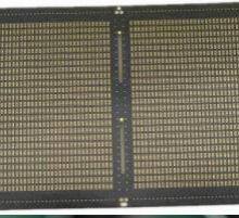
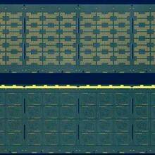
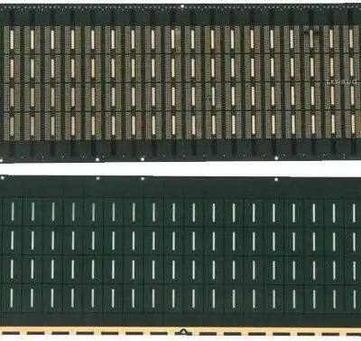
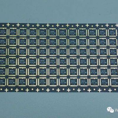
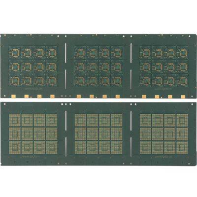
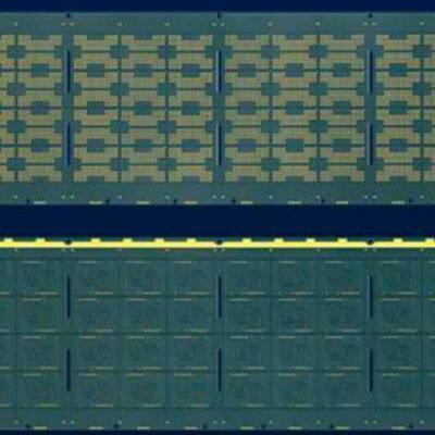
Integrated Chip IC Carrier Board Multi-layer PCB
Product Spotlights
Related Products
-
 16 Layers, Any Order HDI IC Carrier BoardPCB,Bismaleimide TriazinepcbNegotiableMOQ: 1 Blade
 -
14 Layers, Any Order HDI IC Carrier PCB Integrated Chip IC Carrier PCBNegotiableMOQ: 1 Blade
-
14 Layers, Arbitrary Order IC Packaging Substrate PCB,IC Carrier BoardPCBNegotiableMOQ: 1 Blade
-
16layers, Arbitrary Order IC Packaging Substrate PCB,IC Packaging Substrate PCBNegotiableMOQ: 1 Blade
-
12 Layers, 3rd Order, Arbitrary Order IC Packaging Substrate PCBNegotiableMOQ: 1 Blade
If you have any needs, please feel free to contact China Chaosheng Electronics Company. Please contact us as follows:
whatsapp:+8613528819118
Skype live: pcb-fpcb88@163.com
E-mail : sales@chaoshengpcb-fpc.com
Contact: Mank. Li
IC carrier board, single-layer IC carrier board PCB, double-layer IC carrier board PCB, multi-layer IC carrier board PCB, HDIIC carrier board PCB, any order IC carrier board PCB,IC Package Substrapcbtpcb,Ajinomoto Build-up FilmPCB
Bismaleimide Triazinepcb
Introduction to the Production Process Technology of IC Package Substrate by China Chaosheng Electronics
1、 What is an IC carrier board?
**IC packaging substrate=chip "foundation+bridge"
** -Upper end: Connect chip die -Bottom end: soldered to the motherboard PCB -Features:
* * Ultra fine line, ultra-high density, high precision, low loss, high reliability** Hierarchical relationship: Chip → IC Substrate → Motherboard PCB
2、 The three mainstream types of IC carrier boards
1. * * BT resin carrier board (mainstream)
** Used for: CPU, GPU, logic chip, consumer packaging
2. * * ABF laminated carrier board (high-end)
** Used for: HBM, AI computing power, 2.5D/3D, Chiplet
3. * * Ceramic Carrier Board (HTCC/LTCC/AlN)
** Used for: RF, power devices, automotive high voltage
3、 Core process flow of IC carrier board (standard production line)
1. Substrate cutting and pretreatment -Ultra thin substrate: 0.2-0.6mm -Low CTE, high Tg, low Dk/Df -Surface roughening, decontamination, and cleanliness control (cleanroom Class 1000)
2. Inner layer circuit (made of Core) -Thin copper foil (1/3 oz, Ultra thin copper) -LDI laser exposure
* * (without using film)** -Ultra fine etching:
**Ordinary PCB: 50 μ m/50 μ m
** **IC carrier board: 8 μ m/8 μ m, 5 μ m/5 μ m** -AOI 100% inspection for line width, open circuit, and gap
3. Compression (multi-layer laminated board) -Vacuum compression, low tension, low expansion and contraction -Alignment accuracy within ± 25 μ m -Prevent layer deviation and warping (IC carrier board taboo)
4. Micro hole processing (key barrier) Two types of drilling: -UV laser drilling →
* * micro blind hole 30-50 μ m
** -CO ₂ laser drilling → larger blind holes Features: -No dust, smooth pore wall -In the future, all copper should be filled in (ordinary PCBs do not need to be filled in)
5. Copper filling electroplating (the core process) Ordinary PCB: thin electroplating only IC carrier board:
* * VIP vertical hole filling, 100% filling
** Purpose: -Low impedance -High heat dissipation -Air raid shelters, anti breakage measures
6. Outer precision circuit (SAP/MSAP process) Essential for high-end carrier boards:
-* * Reduction method → Improved semi additive MSAP → Fully additive SAP
** Line width limit: - MSAP:5μm -SAP: 2 μ m (for AI and HBM carrier boards)
7. Surface treatment (packaging specific) Not just ordinary gold! -ENEPIG (nickel palladium)
* * mainstream Anti black disk, suitable for gold/copper wire binding -A small amount of OSP and tin deposition
8. Solder mask&characters -Ultra thin solder mask, high-resolution exposure -Do not open large windows to prevent adhesive overflow from affecting chip bonding
9. Shape cutting&splitting -Precision cutting, reducing stress -Control warpage ≤ 0.3%
10. Electrical testing&functional testing -Flying needle/specialized fixture -Full detection of high resistance, micro open circuit, and micro short circuit -Impedance testing, SI/PI electrical verification
11. Full inspection of appearance -AOI+Micron level Optics -X-Ray inspection of copper filling and interlayer defects
4、 IC carrier board vs ordinary PCB (easy to understand at a glance) |Project | Ordinary PCB | IC Packaging Carrier Board| |L/S line width and spacing | 30-100 μ m | 5-10 μ m (advanced 2 μ m)| |Micro porous | 75-200 μ m | 30-50 μ m micro blind hole| |Copper hole | Thin electroplating |
* * Fully filled copper electroplating
* *| |Materials | FR-4 | BT/ABF/High Speed Materials| |Accuracy | ± 75 μ m | ± 20-25 μ m| |Surface treatment | ENIG/OSP |
* * ENEPIG mainly
* *| |Application | Motherboard, Module | CPU/GPU/HBM/AI Chip Packaging| |Workshop level | Class 10000 | Class 1000/Class 100 dust-free|
5、 Key technical barriers to high-end IC carrier boards (industry bottlenecks)
1. * * ABF materials and lamination process (Japanese companies monopolize and gradually produce domestically)
** 2. SAP/MSAP ultrafine line capability**
3. High precision laser micro hole and copper filling yield**
4. * * Low warpage, low CTE control
** 5. * * Extremely low dielectric loss (high frequency and high speed)
** 6. * * Package level cleanliness, ion migration prevention and CAF**
6、 Typical application scenarios -AI server GPU carrier board (ABF high-level number) -HBM high bandwidth memory carrier board -Drone/Autonomous Driving FPGA Carrier Board -Mobile AP, computing chip, RF IC -Automotive power devices, SiP system packaging
7、 Here is a refined keyword for you (suitable for PPT/promotion) IC Substrate、BT/ABF、MSAP/SAP、 Micro line L/S, Microvia micropores, copper filled electroplating, low CTE, high Tg, low Dk/Df, layer alignment ENEPIG、 Warping control, dust-free process, RDL rewiring Fan-out、2.5D/3D、Chiplet、HBM

Send Inquiry to This Supplier


You May Also Like
-
10 Layers, 5th Order, Arbitrary Order IC Packaging Substrate PCBNegotiableMOQ: 1 Blade
-
Multi Layer HDI Server IC Carrier PCB,IC Package SubstrapcbtpcbNegotiableMOQ: 1 Blade
-
6-layer Arbitrary Order Mobile Phone Battery Multi-layer PCBNegotiableMOQ: 1 Blade
-
Antimony Blind Gong HDI Multi-layer PCB,HDI High-frequency High-speed Material PCBNegotiableMOQ: 1 Blade
-
Double Layer Transparent FR-4PCB,Multi Layer FR-4 Transparent PCB,Is the Cost of Producing Multi-layer Transparent CircuitNegotiableMOQ: 1 Unit
-
6L Flexible FPC Second OrderNegotiableMOQ: 1 Unit
-
10L Flexible FPC Second StageFPC,Single Layer Roll to Roll Flexible FPCNegotiableMOQ: 1 Unit
-
10 Layer Third-order HDI Flexible FPC,multi-layer Ultra Large Flexible FPCNegotiableMOQ: 1 Unit
-
Fake Double-layer Floor Hollow FPC, Pure Copper Based Floor Hole FPC,Multi Layer Flexible FPCNegotiableMOQ: 1 Unit
-
Transparent FR-4PCB,FR-4, TG130 Material,PI Transparent Flexible Board FPCNegotiableMOQ: 1 Unit


