

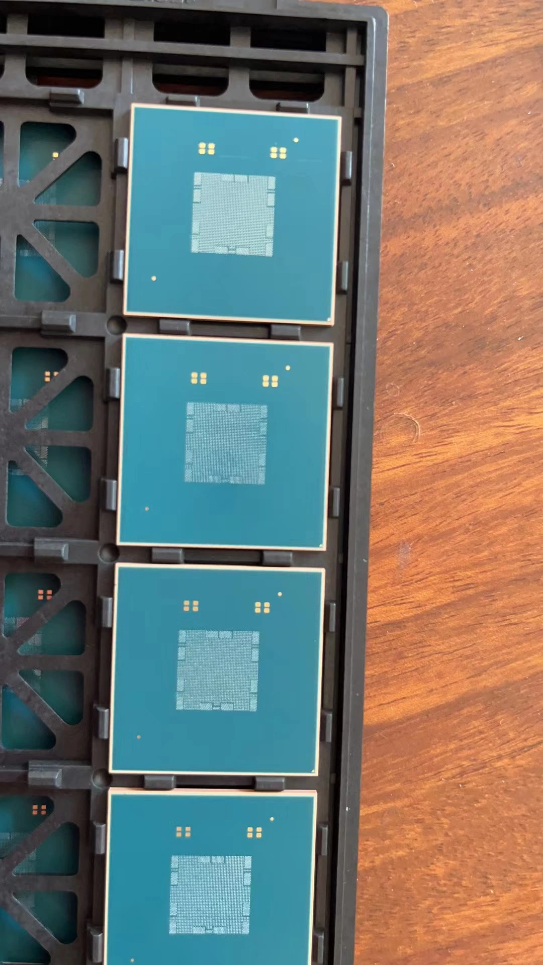
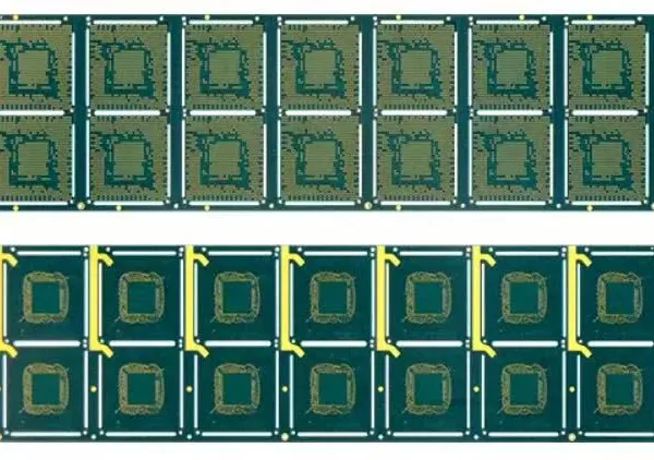
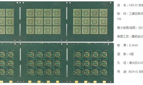
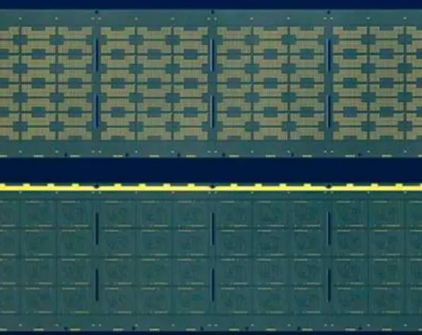
10 Layers, 5th Order, Arbitrary Order IC Packaging Substrate PCB
Product Spotlights
Related Products
-
 Multi Layer HDI Server IC Carrier PCB,IC Package SubstrapcbtpcbNegotiableMOQ: 1 Blade
 -
Integrated Chip IC Carrier Board Multi-layer PCBNegotiableMOQ: 1 Blade
-
16 Layers, Any Order HDI IC Carrier BoardPCB,Bismaleimide TriazinepcbNegotiableMOQ: 1 Blade
-
14 Layers, Any Order HDI IC Carrier PCB Integrated Chip IC Carrier PCBNegotiableMOQ: 1 Blade
-
14 Layers, Arbitrary Order IC Packaging Substrate PCB,IC Carrier BoardPCBNegotiableMOQ: 1 Blade
If you have any needs, please feel free to contact China Chaosheng Electronics Company. Please contact us as follows:
whatsapp:+8613528819118
Skype live: pcb-fpcb88@163.com
E-mail : sales@chaoshengpcb-fpc.com
Contact: Mank. Li
Product Name: IC Packaging Carrier Board
Material: Japanese 705G+Japanese Mitsubishi BT832
Layers: 10 layers, 5th order, arbitrary order IC packaging substrate PCB
Minimum line width/spacing: 15um/15um
Finished product size: 17 * 17mm
Surface technology: Nickel palladium gold
Copper thickness: 18um
Plate thickness: 1.60mm
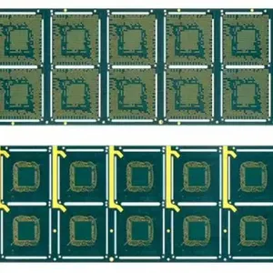
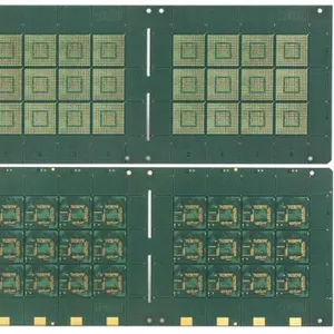
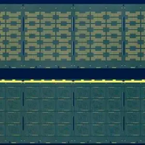
Features: Integrated circuit, minimum wire size of 15um, ultra-thin, is a high-end IC substrate. As a high-end PCB (printed circuit board), it is a key bridge between integrated circuits (IC) and external circuits. Its core function is to achieve electrical connection, physical support, and functional coordination between IC chips and downstream electronic devices. It is an indispensable product in the electronics industry.
IC carrier board is the "high-end interface" that connects IC chips with external circuits. Its core function is to achieve stable output of chip functions through high-density electrical connections, physical support and protection, heat dissipation assistance, and signal integrity optimization. It is an indispensable key component in high-end electronic devices such as smartphones, computers, 5G communication, and artificial intelligence. With the improvement of chip integration (such as 3nm and 2nm processes), the circuit density and performance requirements of IC carrier boards are constantly increasing, becoming one of the high technical barriers in the semiconductor industry chain
Usage: Automotive lights LED、 High end chips such as computers, medical devices, mobile phones, artificial intelligence, AI, etc
Packaging substrate: IC carrier board, also known as packaging substrate, is developed on the basis of PCB board related technology, used to establish signal connections between IC and PCB, and is a key substrate for advanced packaging of integrated circuits.
High density: IC carrier boards have the characteristic of high density and need to meet the requirements of high-density integrated circuit packaging, such as high-density wiring, to achieve effective connection between chips and other components.
High precision: It requires high precision, strict requirements in terms of fine circuit, hole spacing size, and signal interference, and requires highly precise interlayer alignment technology, electroplating capability, drilling technology, etc.
High performance: With high temperature resistance and high-frequency performance, it can support the high-speed computing and data processing needs of more electronic devices in the future, providing stable electrical connections and good heat dissipation for chips.
Miniaturization and thinning: As a high-end PCB board, IC carrier boards have the characteristics of miniaturization and thinning to adapt to the development trend of modern electronic products being lightweight and portable.
Multi layer structure: Typically designed with multiple layers, it can support designs with 2 to 12 or even more layers. The more layers there are, the better the performance and meet the needs of different chip packaging.
Signal transmission: Ensuring efficient transmission of electrical signals is an important function of IC boards. To meet the requirements of high-speed signal transmission, optimized impedance control is needed to ensure stable signal transmission and low attenuation.
Thermal management: IC carrier boards usually need to cope with high operating temperatures, and thermal management is emphasized in design. Effective heat dissipation is achieved through special materials and structural design to extend component life.
Surface treatment: There are various surface treatment methods, such as immersion gold, OSP, HASL, etc., to meet different environmental and electrical performance requirements.
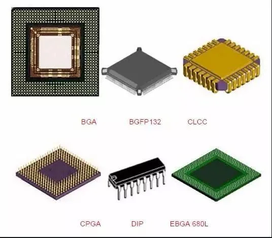
Packaging materials: According to different packaging materials, IC carrier boards can be divided into hard packaging substrates, flexible packaging substrates, and ceramic packaging substrates. The main materials for hard substrates are BT resin, ABF resin, MIS, etc.
Packaging process: Common packaging processes include wire bonding and flip chip bonding. Wire bonding is widely used in the packaging of RF modules, storage chips, and microelectromechanical system devices; Inverted packaging is widely used in the packaging of products such as CPUs, GPUs, and Chipsets.
Industry barriers: IC board manufacturing faces triple barriers of capital, technology, and customers, with high technical barriers and significant difficulties in research and mass production.
Application areas: Widely used in communication, computer, mobile terminal, industrial control and medical, automotive electronics, aerospace and other fields, different fields have their own characteristics in terms of the performance and requirements of IC carrier boards.
Chaosheng Group has significant advantages in IC board technology and quality. The following is a detailed introduction:
Technical aspects
Advanced process technology: Chaosheng Group has advanced blind gong and blind groove technology, which can ensure the precise connection of internal circuits of IC carrier boards, which is of great significance for the production of multi-layer boards and can meet the requirements of high-density circuit layout. At the same time, the surface of the circuit board is treated with immersion gold technology to present a uniform and bright golden color, which improves the oxidation resistance and conductivity, and is conducive to the reliable connection between the IC carrier board and chips and other components.
Rich product layer design capability: Its PCB business can achieve the production of 2-100 layer circuit boards. This extensive layer design capability can meet the needs of IC carrier boards with different levels of complexity, from simple double-layer carrier boards to highly complex multi-layer carrier boards, all within the production capacity range of Chaosheng Group.
High precision drilling technology: For the processing of small holes on IC substrates, Chaosheng Group adopts laser drilling technology, which can achieve high-precision small hole processing and meet the design requirements of dense circuits and small PAD pads. Its BT circuit board PAD is less than 15 microns, and the finished board thickness is ultra-thin, reaching 0.1 to 0.3 millimeters, reflecting its superb technical level in drilling and overall processing accuracy.
Material application and processing technology: Chaosheng Group uses special BT materials in IC board production, such as materials with high resin content and stable performance, which can prevent interference and withstand high temperatures of over 260 degrees Celsius. At the same time, the original resin plug holes were replaced with direct copper filling nickel palladium gold and other processes, optimizing the PCBA process structure, improving the heat dissipation of the product, reducing the expansion and contraction coefficient, and enhancing the performance and stability of the IC carrier board.
Automated production technology: Chaosheng Group's IC board factory in Japan has an automation production level of over 90%. Advanced automated production equipment and technology can improve production efficiency, ensure consistency and stability of product quality, and reduce the impact of human factors on product quality.
In terms of quality
A sound quality management system: The company has IE, ERP, Six Sigma, ISO quality management systems, and has passed quality system certifications such as UL, ISO9001, TS16949, ISO14000, QS8000 in the United States. From raw material procurement, production process control to finished product inspection, there are strict quality control processes to ensure that product quality meets international standards and customer requirements.
Strict testing process: Chaosheng Group is equipped with advanced AOI optical testing X - ray、 Optical automatic testing equipment and finished product function testing racks are used to conduct comprehensive inspections of IC carrier boards, including visual inspection, internal circuit testing, electrical performance testing, reliability testing, etc., to ensure that each IC carrier board meets quality standards and the product quality is stable and reliable.
Wide market recognition: Chaosheng Group's products are widely used in high-tech fields such as communication equipment, intelligent systems, new energy, medical devices, aerospace, etc. These fields have extremely high requirements for product quality. Chaosheng Group's ability to meet the needs of these fields indicates that the quality of its IC carrier board products has been widely recognized by the market.
Strong production strength guarantee: Chaosheng Group's annual output value exceeds 100 billion yuan, the annual output value of printed circuit boards reaches over 35 billion yuan, and the monthly production capacity reaches 650000 square meters. Strong production strength means that there are sufficient resources and capabilities to invest in quality control and ensure timely delivery of products, further reflecting the reliability of its product quality.
|
Process Capability Table | ||||
| Technical ltem | MassProduct | Advanced Technology | ||
| 2015 | 2021 | 2025 | ||
| Max.Layer Count | 80 layer | 100 layer | 100 layer | |
|
PCB through hole board |
2~80 layer | 2~100 layer | 2~100 layer | |
|
Maximum size through hole 1~2 |
37〞*98.50" | 43.3〞*118.11" | 43.3〞*118.11" | |
|
Minimum line width and spacing |
10(0.40) | 10(0.40) | 7.50(0.30mm) | |
| Minimum mechanical hole(mm) |
12(0.50) | 10(0.40) | 8.50(0.35mm) | |
|
Maximum size through hole 4~22 layers |
37〞*43.30" | 43.3〞*43.30" | 43.3〞*43.30" | |
|
Maximum size through hole 4~22 layers |
31.50 ″*59" | 31.50 ″*70.86" | 31.50 ″*70.86" | |
|
Maximum size through hole 4~22 layers |
10(0.40) | 10(0.40) | 7.50(0.30mm) | |
| Minimum line width and spacing for multi-layer large-sized PCBs |
10(0.40) | 10(0.40) | 7.50(0.30mm) | |
|
Maximum size of multi-layer through- hole : 4-22 layers with the smallest hole |
12(0.50) | 10(0.40) | 8.50(0.35mm) | |
| Maximum size HDI 4~36 layers | 31.50 ″*55" | 31.50 ″*55" | 31.50 ″*55" | |
| Minimum line width and line spacing of large size PCB |
Through hole 12 / 12milHDI14 /14mil |
Through hole 10/10 milHDI12 / 12mil |
Through hole 8 / 8milHDI12 / 12mil |
|
| The largest board ruler 1 → the smallest hole of 18 layers |
Through hole 0.50mmHDI :0.45mm |
Through hole 0.50mm HDI : 0.45mm |
Through hole 0.50mmHDI : 0.45mm |
|
| The layer number of FPC | 1~36layer | 1~60layer | 1~60layer | |
| Maximum size of flexible FPC |
19.68〞*55" | 28〞*59" | 31.49〞*118.12" | |
| Maximum size of flexible FPC with soft hard combination |
19.68〞*55" | 28〞*59" | 31.49〞*118.12" | |
|
FPC (roll to roll) maximum size |
19.68 ″*7874" | 19.68 ″*7874" | 19.68 ″*7874" | |
|
Maximum size of FPC single chip shipment |
19.68 ″*118.11" | 19.68 ″*196.8" | 19.68 ″*196.80" | |
| The layer number of FPC | 2~18 layer | 2~36 layer | 2~42 layer | |
|
Maximum size of layered board |
19.68 ″*35" | 19.68 ″*43" | 19.68 ″*43" | |
|
Number of through-hole layers |
2~20layer | 2~30 layer | 2~40 layer | |
|
Hard and soft HDI layers |
2~14 layer | 2~18 layer | 2~22 layer | |
|
Maximum size of soft and hard combination |
19.68 ″*43" | 19.68 ″*49" | 19.68 ″*49" | |
|
FPC/soft-hard combination arbitrary interconnection HDI |
4+X+4Interconnect HDI |
5+X+5Interconnect HDI | 6+X+6Interconnect HDI |
|
|
HDIPCB layers |
4~36layer | 4~60layer | 4~80 layer | |
|
Anylayer HDI PCB |
4+X+4Interconnect HDI |
5+X+5、Interconnect HDI | 8+X+8、Interconnect HDI |
|
|
HDIPCB maximum board size |
24"*52" | 43"*49" | 43"*49" | |
|
Number of through hole layers of high frequency board |
2~18 layer | 2~36 layer | 2~60 layer | |
| HDI layers ofhighfrequency board |
2~16 layer | 2~24 layer | 2~60layer | |
| Maximum size of high frequency board |
37 ″*43" | 43 ″*49" | 43 ″*49" | |
|
Number of ceramic plates |
1-2 layer | 1~4 layer | 1~6 layer | |
|
Ceramic plate thickness |
0.60mm-1.60mm | 0.38mm-20.0mm | 0.38mm-20.0mm | |
|
Maximum size of ceramic plate |
100*150mm | 150*190mm | 150*650mm | |
|
Minimum aperture of ceramic plate |
0.50mm | 0.35mm | 0.35mm | |
|
Minimum line width and line spacing of ceramic board |
16/16mil | 12/12mil | 10/10mil | |
|
Number of layers of metal copper substrate |
1-2 layer | 1~4 layer | 1~6 layer | |
|
Maximum line width and line spacing of metal iron substrate |
12/12mil | 4/4mil | 4/4mil | |
|
Number of layers of metal aluminum substrateHDI |
1-2 layer | 1~4 layer | 1~6 layer | |
|
Maximum size of metal substrate |
37 ″*43" | 25.59 ″*59" | 25.59 ″*59" | |
| The smallest hole of the metal substrate |
0.50mm | 0.35mm | 0.35mm | |
|
Minimum line width and line spacing of metal substrate |
8/8mil | 4/4mil | 4/4mil | |
| Transparent FR- 4 material layers |
1-2layer | 1-2layer | 1-8layer | |
| Transparent FR-4 minimum hole |
0.35mm | 0.35mm | 0.35mm | |
| Transparent FR-4 minimum line width and spacing |
4/4Mil | 4/4Mil | 3.5/3.5Mil | |
| Transparent FR- 4 maximum size |
23.63*47.25″ | 23.63*47.25 ″ | 23.63*47.25 ″ | |
| Number of tempered glass base layers |
1-2layer | 1-2layer | 1-2layer | |
| Minimum line width and spacing of glass |
4/4Mil | 4/4Mil | 3.5/3.5Mil | |
| The smallest hole in glass |
0.35mm | 0.35mm | 0.35mm | |
| Maximum size of glass |
23.63*47.25″ | 23.63*47.25 ″ | 23.63*47.25 ″ | |
| Number of layers of transparent PETmaterial |
1-2layer | 1-2layer | 1-2layer | |
| Maximum size of transparent PET |
19.68 ″*7874" | 19.68 ″*7874" | 19.68 ″*7874" | |
|
The company's main product types |
Halogen free materials, high TG materials, high-frequency materials, high-speed materials, metal materials, glass materials, embedded materials, transparent FR- 4 materials, high thermal conductivity metals, high thermal conductivity aluminum substrates, environmentally friendly circuit boards, BT materials, ABF materials, and other imported materials, DU busbars, iron-based and metal based (core) mixed pressure plates, embedded buried copper, buried resistors, buried capacitors, buried ceramic bead plates, buried ceramics, ceramic mixed pressure plates, multi-layer ceramics, ultra-thin BT plates, ultra-thin PCBs, ultra-thin PCBs, multi-layer aluminum substrates, multi-layer ceramic plates, multi-layer ultra-thin HDI、 High frequency mixed voltage, differential impedance board, thick copper plate, gold-plated plate, high and low copper, high and low copper, high carbon resistance, transparent multilayer, glass plate, HDI arbitrary order (cross blind buried) Anylayer, flexible double-sided, flexible multilayer, soft hard combination HDI, roll to roll FPC, ultra long size, ultra large size board (single, double, multi-layer) PCB production and product design, product development, software development, etc |
|||
| Main material |
Rogers, Taikoni, Yaron, Mitsui, Isola, 3M, Taiyao, Taiguang, Tenghui, Shengyi,Lianmao, Nanya, Doosan, DuPont, Taihong, Hongren, Xinyang, Nippon Steel, Teflon,Yasen, Panasonic, RCC, Mitsui, Mitsubishi, Yingye, 3M, Kyocera, Jiuhao, Zhongci,Huaqing, Aishengda, Sliton, Kaichangde, Tongxin, Beige, Yalong, Taikoni,Hitachi, Laird System, etc |
|||
|
Main material categories |
Halogen-free、halogenated、 high thermal conductivity, high TG135 、TG140、 TG150、 TG170、TG180、TG240、TG320 |
|||
| Build-up Material | FR-4 ,TG150,TG70,TG180 | |||
| Conventional plate thickness (mm) |
Min.1-2L(mm) | 0.10mm | 0.10-12.0mm | 0.10-18.0mm |
| Min.4-10L(mm) | 0.35mm | 0.35mm~10.0mm | 0.35-18.0mm | |
| Min.12L(mm) | 0.43 | 0.38~10.0mm | 0.38~18.0mm | |
| Min.16L(mm) | 0.53 | 0.45~10.0mm | 0.45~18.0mm | |
| Min.18L(mm) | 0.63 | 0.51~10.0mm | 0.51~18.0mm | |
| Min.52L(mm) | 0.8 | 0.65~10.0mm | 0.65~18.0mm | |
| MAX(mm) | 3.5 | 12.0mm | 18.0mm | |
|
Copper plate thickness and copper thickness |
1-2 layerCU | 700um | 875um | 875um |
| Layers 4-20 |
4-12layer | 4-16layer | 4-22layer | |
| Inner layer copper thickness(um) |
875um | 1050um | 1225um | |
|
Outercopperthickness |
210um | 350um | 525um | |
|
Thick copper finished plate thickness |
8.0mm | 12.0mm | 18.0mm | |
| IC substrate |
layerHDI | 1-10layer | 1-14layer | 1-16layer |
| Line width and spacing |
50um | 25um | 15um | |
| copper thickness |
8-10um | 10-12um | 12-15um | |
| Min.CoreThickness um(mil) | 254" (10.0) | 0.15~254(10.0mm) | 0.15~254(10.0mm) | |
| Min.Build up Dielectric |
38(1.5) | 25(1.0) | 25(1.0) | |
|
BaseCopperWeigh t |
Inner Layer | 1/4-8 OZ | 1/4-0.30mm | 1/4-0.30mm |
| Out Layer | 1/4-10 OZ | 1/4-30 OZ | 1/4-30 OZ | |
| Gold thick | 1~40u" | 1~200u" | 1~200u" | |
| Nithick | 76~127u" | 1~250u" | 1~250u" | |
|
Min.HOle/Land um(mil) |
150/300(6/12) | 100/200(4/8) | 100/200(4/8) | |
|
Min.Laser via/landum(mil) |
60/170(2.4/6.8) | 50/150(2/6) | 50/150(2/6) | |
|
Min. IVH、Hole size/landum(mil) |
150/300(6/12) | 100/200(4/8) | 100/200(4/8) | |
| DieletricThickness | 38(1.5) | 32(1.3) | 32(1.3) | |
| 125(5) | 125(5) | 125(5) | ||
| SKipvia | Yes | Yes | Yes | |
| viaoNhie(laserviaon BuriedPTH) | Yes | Yes | Yes | |
| Laser Hole Filling | Yes | Yes | Yes | |
| Technicalltem | MassProduct | Advanced Technology | ||
| Hole depth/diameter | Through Hoie | 25:01 :00 | 35:01 :00 | 40:01 :00 |
| AspctRatio | MicroVia | 0.8 :1 | 0.8 :1 | 0.8 :1 |
| copperFilling Dimple Size | 10(0.40) | 5(0.20) | 5(0.20) | |
|
Minimumouter line width/ spacing |
Inner layer line width and spacing | 38/38(1.5/1.5) | 38/38(1.5/1.5) | 38/38(1.5/1.5) |
|
PlatedLayerum(mil) |
38/38(1.5/1.5) | 38/38(1.5/1.5) | 38/38(1.5/1.5) | |
| BGAPitchmm(mil) | 0.4 | 0.4 | 0.4 | |
| PHMin.Hole rlng um(mil) | 75(3) | 62.50(2.50 | 62.50(2.50 | |
| Line Width control |
±0.50 | ±0.50 | ±0.50 | |
| 2.5mil≤L/W | ±0.50 | ±0.50 | ±0.50 | |
| ≤3mil(mil) | ±0.60 | ±0.60 | ±0.60 | |
| SolderMask Registration um(mil) |
±25 | ±25 | ±25 | |
| Solder masThickness |
Lines Minum(mil) | 10(0.40) | 10(0.40) | 10(0.40) |
| Lines Minum(mil) | 30(1.20) | 30(1.20) | 30(1.20) | |
| CopperMinum(mil) | 10(0.40) | 10(0.40) | 10(0.40) | |
| CopperMax um(mil) |
30(1.20) | 30(1.20) | 30(1.20) | |
| Mln.Solder Mask opening um(mil) |
250(10) | 200(8) | 200(8) | |
|
Structure |
Stacking layer by layer |
5+N+5 | 6+N+6 | 7+N+7 |
| Sequenetlal Bu il-up | 42Any Layer | 46Any Layer | 60Any Layer | |
| Stacking layer by layer |
N+N | N+N | N+N | |
| N+X+N | N+X+N | N+X+N | ||
| Sequenetlal Lamination |
4+(N+X+N)+4 | 5+(N+X+N)+5 | 6+(N+X+N)+6 | |
|
Multi-layer stepped structure |
Multi- layer stacking |
5+N+5 | 6+N+6 | 7+N+7 |
| Sequenetlal Bu il-up | 12Any Layer | 16Any Layer | 18Any Layer | |
| Multi- layer staircase |
4 steps | 6 steps | 6 steps | |
| Mechanical depth control drilling depth |
2.0mm±0.08mm | 2.0mm±0.08m | 2.0mm±0.08m | |
| Laser controlled depth drilling |
0.6mm±0.08mm | 0.8mm±0.08mm | 1.0mm±0.08mm | |
|
/Min.HOle/Land um(mil) |
linner um(mil) | 150/300(6/12) | 100/200(4/8) | 100/200(4/8) |
| Outer um(mil) | 150/300(6/12) | 100/200(4/8) | 100/200(4/8) | |
|
Minimumburiedholediameter/solder pad |
60/170(2.4/6.8) | 50/150(2/6) | 50/150(2/6) | |
| SUBDielectricThic kness |
Mln.um(mil) | 38(1.5) | 32(1.3) | 25(1.0) |
| Max.um(mil) | 125(5) | 125(5) | 125(5) | |
| SKipvia | Yes | Yes | Yes | |
| Via on hole(LaserViaon BuriePTH | Yes | Yes | Yes | |
| Laser Hole Filling | Yes | Yes | Yes | |
|
Resin plug hole plate thickness |
Min mm(mil) | 0.35 | 0.35 | 0.35 |
| Max mm(mil) | 3.2 | 3.2 | 3.2 | |
| Min mm(mil) | 125(5) | 110(4.50) | 110(4.50) | |
| Routing Depth control Accuracy um(mil) |
±50um(mil) | ±50um(mil) | ±50um(mil) | |
| Outine NC Rcuting Tolerance um(mil) |
75(3) | 75(3) | 75(3) | |
|
Type of surface Finishing |
OSP、 Sinking gold, lead-free tin, lead tin, electroplated gold fingers, electroplated gold (electroplated nickel hard gold, electroplated nickel soft gold), gold fingers+sinking gold, spray tin+gold fingers, OSP+electroplated gold, OSP+sinking gold, electroplated silver, electroplated silver, electroplated tin, gold coated silver, nickel free electroplated thick gold, nickel free electroplated thick silver, tin silver copper, OSP+gold fingers |
|||
| EN Thickness Control(um) |
>0.025-0.1um | >0.025-0.1um | >0.025-0.1um | |
| OSOSP Thickness(um) | >0.20-0.50um | >0.20-0.50um | >0.20-0.50um | |
| Ni Thickness(um) |
>105⇢ 250um | >105⇢ 250um | >105⇢ 250um | |
| Platinum thickness control |
>0.025-5um | >0.025-5um | >0.025-5um | |
| Lead/lead- free tin spraying thickness |
>105⇢ 150um | >105⇢ 150um | >105⇢ 150um | |
| Electrosilver | >105⇢ 140um | >105⇢ 140um | >105⇢ 140um | |
| Thickness control of sinking silver |
>105⇢ 140um | >105⇢ 140um | >105⇢ 140um | |
| Tin thickness control |
>105⇢ 140um | >105⇢ 140um | >105⇢ 140um | |
|
Min TestPAD |
E/Tum(mil) | 75(3) | 75(3) | 75(3) |
| E/Tum(mil) | 50(2) | 50(2) | 50(2) | |
| E/Tum(mil | 25(1) | 25(1) | 25(1) | |
| E/Tum(mil) | 150(6) | 150(6) | 150(6) | |
|
lmpedanceContro lTolerance |
≧50ohm | ± 10% | ±8% | ±8% |
| ≦50ohm | ±50ohm | ±50ohm | ±50ohm | |
| Finished board | Plate thickness≧0.15mm | ≧ ± 10% | ≧ ± 10% | ≧ ± 10% |
| Plate thickness≧0.15mm | ≧ ±0.075% | ≧ ±0.075% | ≧ ±0.075% | |
| Warpage | ≤0.7% | ≤0.5% | ≤0.5% | |
| The above are the conventional production skills of Chaosheng Group Company, and there are any unclear points. Please further communicate with our specialized technical personnel, and we will be happy to serve you! Welcome to our guide! | ||||
| FAQ | |||||||||||||||||||
| Serial Number | Question Point | Answer | |||||||||||||||||
| Q1 | Q: What information is required to make a PCB | CEGSATE: Gberber files for PCB production, product process instructions, such as material requirements, surface treatment requirements, finished product thickness requirements, PCB stack structure diagram for advanced products, copper thickness requirements for each layer, sample quantity requirements, batch order requirements, product application fields, and other related information are required | |||||||||||||||||
| Q2 | Q: What information does PCBA need to provide | CEGSATE: BOM report is required (including the brand, specifications, and model of the components), X and Y coordinate numbers of PCBA components, and processing requirements: Do we need to purchase the components on our behalf? Or customer supplied components? Do you need software burning? What is the required quantity? What is the monthly demand and other detailed information. | |||||||||||||||||
| Q3 | Question: Is my file secure? | CEGSATE: Your files are very secure, and we protect intellectual property rights for our clients throughout the entire process. All files provided by the customer will never be shared with any third party. | |||||||||||||||||
| Q4 | Q: What is the minimum order quantity? | CESGATE: We do not have a minimum order quantity for PO orders. We are able to handle small and large batches flexibly. | |||||||||||||||||
| Q5 | Q: What is your inspection method? How do you control the quality? | CESGATE: In order to ensure the quality of PCB, FPC, and PCBA products, we use flying pin testing for small batches, which is usually used for samples and small batches; The inner circuit undergoes 100% optical inspection through AOI, and we have online AOI automatic inspection for intermediate inspection. Batch finished products undergo 100% inspection through E-SET testing rack. The appearance is 100% inspected by fully automated finished product testing equipment and FQC. PCBA undergoes automatic optical inspection (AOI), 100% X-ray inspection of BGA parts, and first article inspection (FAI). PCBA products that require software burning must undergo 100% comprehensive testing on the finished product testing rack according to product functional requirements before they can be shipped. |
|||||||||||||||||
| Q6 | Q: What standard should PCB be shipped according to? | WCESGATE: e accept and store according to the international IPC-6012 Level 2 standard. If there are special requirements for Level 3 standards in the quotation, we accept and store according to the international IPC-6012 Level 3 standardWe accept and store according to the international IPC-6012 Level 2 standard. If there are special requirements for Level 3 standards in the quotation, we accept and store according to the international IPC-6012 Level 3 standard | |||||||||||||||||
| Q7 | Q: May I ask how you package and ship? | 1:PCBVacuum packaging+separated white paper+moisture-proof beads+cardboard box 2:PCBVacuum packaging+white paper insulation+moisture-proof beads+tin vacuum packaging+cardboard box 3:PCBSpecial size PCB, vacuum packaging+separated white paper+moisture-proof beads+wooden frame or plastic bag packaging+separated white paper+moisture-proof beads+wooden frame 4: PCBA anti-static packaging 5: PCBA anti-static film+vacuum box packaging+shelving |
|||||||||||||||||

Send Inquiry to This Supplier

You May Also Like
-
16layers, Arbitrary Order IC Packaging Substrate PCB,IC Packaging Substrate PCBNegotiableMOQ: 1 Blade
-
12 Layers, 3rd Order, Arbitrary Order IC Packaging Substrate PCBNegotiableMOQ: 1 Blade
-
8 Layers HDIPCBNegotiableMOQ: 1 Blade
-
16 Layer HDI Automotive Product PCBA,AI Communication Server PCBNegotiableMOQ: 1 Blade
-
42 Layers HDI Automotive Product PCBANegotiableMOQ: 1 Blade
-
48layer HDI Automotive Product PCBA,10 Layer HDI Arbitrary Order HDIPCBANegotiableMOQ: 1 Blade
-
10 Layers HDI Automotive Product PCBA,80 Layer Communication Server PCBANegotiableMOQ: 1 Blade
-
50layer HDI Automotive Product PCBA,18 Layer Intelligent Product PCBANegotiableMOQ: 1 Blade
-
P0.937MiLED8 Layer 3rd Order HDIPCB,MiNiLEDHDIPCBNegotiableMOQ: 1 Blade
-
P0.925, INiLED8 Layer, 3rd Order HDIPCB,MiNiLEDHDIPCB,OMiNiLEDFPC,NegotiableMOQ: 1 Blade


