

Home > Electrical & Electronics > Circuit Board > Other Circuit Board > 6 Transparent FR-4 Circuit Boards PCB
6 Transparent FR-4 Circuit Boards PCB

Product Spotlights
Transparent PETFPC,Transparent FR-4PCB,Ultra thin transparent FR-4PCB,Transparent PCB display screen,Transparent FR-4PCB display screen,LED transparent screen PCB,Button transparent PET carbon wire FPC,Film switch transparent PET silver wire FPC,Thin film switch FPC,Thin film switch carbon wire FPC,
Negotiable
MOQ: 1 Blade (Price negotiable depending on order volume and customization)
Key Specifications
Get Latest Price
Dielectric:
Other, Transparent FR-4
Transport Package:
vacuum packaging
Specification:
500x1200mm
Payment & Shipping
Payment Methods:
Port of Shipment:
Shenzhen Wendu Port
Delivery Detail:
25 days
Related Products
-
 Transparent Glass Circuit Board PCB, Copper Wiring Transparent Glass PCBNegotiableMOQ: 1 Blade
 -
Transparent Tempered Glass Circuit Board PCB, Copper WiringNegotiableMOQ: 1 Blade
-
Tempered Glass PCB Glass PCBNegotiableMOQ: 1 Blade
-
China Chaosheng Electronics, Fake Double-layer Perforated Flexible FPC, Model CSFPC23650, Ultra-thin, FlexibleNegotiableMOQ: 1 Blade
-
China Super Sheng Twelve Layer HDI Soft Hard Combined FPC, DuPont Material, LCD Display Motherboard Flexible FPCNegotiableMOQ: 1 Blade
Dielectric
Other, Transparent FR-4
Transport Package
vacuum packaging
Specification
500x1200mm
Origin
vacuum packaging
If you have any needs, please contact us:
whatsapp:+8613528819118
Skype live: pcb-fpcb88@163.com
E-mail : sales@chaoshengpcb-fpc.com
Contact: Mank. Li
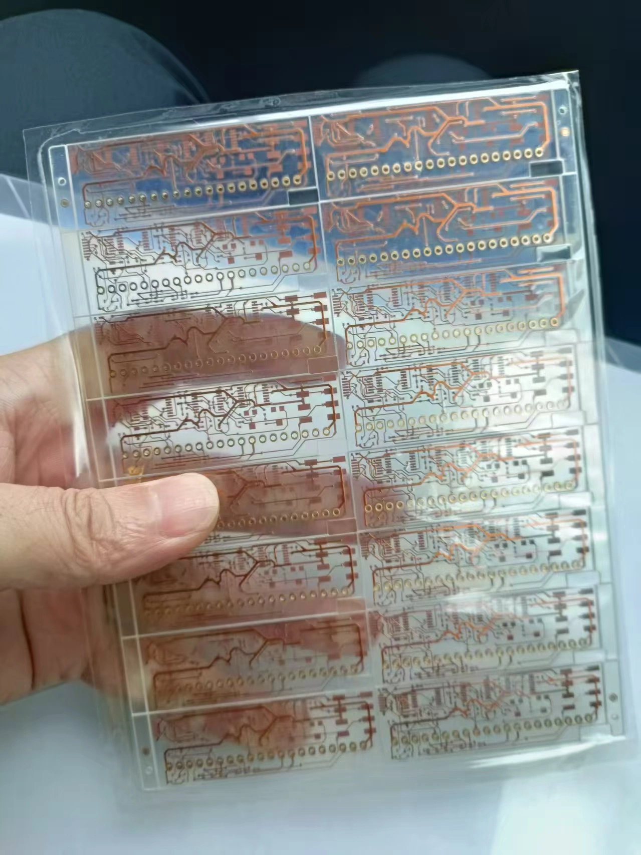
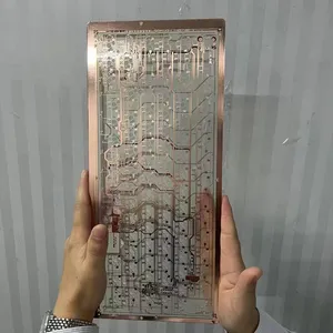
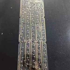
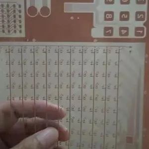
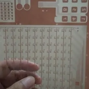
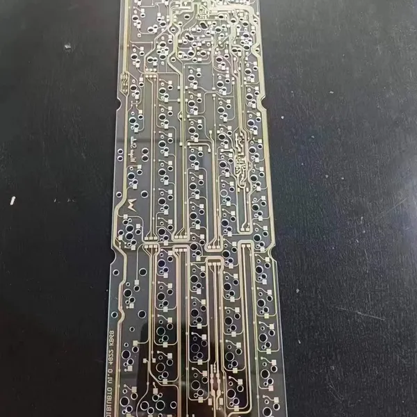
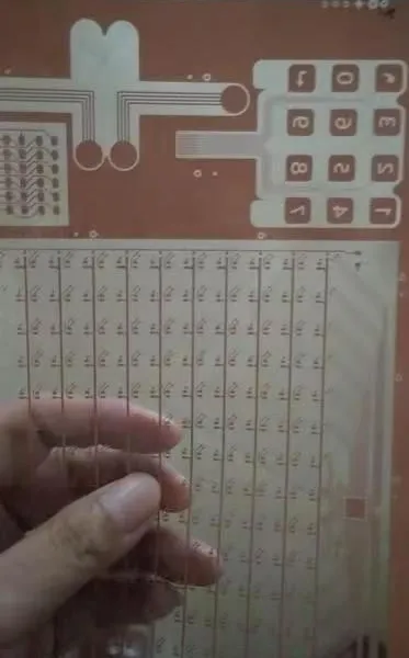
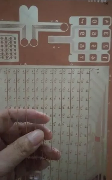
Product Name: Transparent Display Screen
Board: Transparent FR-4
Number of floors: 6 transparent FR-4 circuit boards PCB
Minimum line width/spacing: 8/8mil
Finished product size: 500x1200mm
Surface technology: OSP
Copper thickness: 35
Plate thickness: 0.10-5.0mm
Minimum aperture: 0.35mm
Features: Transparency reaches 85-95% and can withstand normal temperatures of 220-240 degrees Celsius
Usage: Large size, LED transparent screen, display frequency, LED glass screen, film switch, etc
FR-4 multi-layer transparent PCB detailed introduction
|
Process Capability Table | ||||
| Technical ltem | MassProduct | Advanced Technology | ||
| 2015 | 2021 | 2025 | ||
| Max.Layer Count | 80 layer | 100 layer | 100 layer | |
|
PCB through hole board |
2~80 layer | 2~100 layer | 2~100 layer | |
|
Maximum size through hole 1~2 |
37〞*98.50" | 43.3〞*118.11" | 43.3〞*118.11" | |
|
Minimum line width and spacing |
10(0.40) | 10(0.40) | 7.50(0.30mm) | |
| Minimum mechanical hole(mm) |
12(0.50) | 10(0.40) | 8.50(0.35mm) | |
|
Maximum size through hole 4~22 layers |
37〞*43.30" | 43.3〞*43.30" | 43.3〞*43.30" | |
|
Maximum size through hole 4~22 layers |
31.50 ″*59" | 31.50 ″*70.86" | 31.50 ″*70.86" | |
|
Maximum size through hole 4~22 layers |
10(0.40) | 10(0.40) | 7.50(0.30mm) | |
| Minimum line width and spacing for multi-layer large-sized PCBs |
10(0.40) | 10(0.40) | 7.50(0.30mm) | |
|
Maximum size of multi-layer through- hole : 4-22 layers with the smallest hole |
12(0.50) | 10(0.40) | 8.50(0.35mm) | |
| Maximum size HDI 4~36 layers | 31.50 ″*55" | 31.50 ″*55" | 31.50 ″*55" | |
| Minimum line width and line spacing of large size PCB |
Through hole 12 / 12milHDI14 /14mil |
Through hole 10/10 milHDI12 / 12mil |
Through hole 8 / 8milHDI12 / 12mil |
|
| The largest board ruler 1 → the smallest hole of 18 layers |
Through hole 0.50mmHDI :0.45mm |
Through hole 0.50mm HDI : 0.45mm |
Through hole 0.50mmHDI : 0.45mm |
|
| The layer number of FPC | 1~36layer | 1~60layer | 1~60layer | |
| Maximum size of flexible FPC |
19.68〞*55" | 28〞*59" | 31.49〞*118.12" | |
| Maximum size of flexible FPC with soft hard combination |
19.68〞*55" | 28〞*59" | 31.49〞*118.12" | |
|
FPC (roll to roll) maximum size |
19.68 ″*7874" | 19.68 ″*7874" | 19.68 ″*7874" | |
|
Maximum size of FPC single chip shipment |
19.68 ″*118.11" | 19.68 ″*196.8" | 19.68 ″*196.80" | |
| The layer number of FPC | 2~18 layer | 2~36 layer | 2~42 layer | |
|
Maximum size of layered board |
19.68 ″*35" | 19.68 ″*43" | 19.68 ″*43" | |
|
Number of through-hole layers |
2~20layer | 2~30 layer | 2~40 layer | |
|
Hard and soft HDI layers |
2~14 layer | 2~18 layer | 2~22 layer | |
|
Maximum size of soft and hard combination |
19.68 ″*43" | 19.68 ″*49" | 19.68 ″*49" | |
|
FPC/soft-hard combination arbitrary interconnection HDI |
4+X+4Interconnect HDI |
5+X+5Interconnect HDI | 6+X+6Interconnect HDI |
|
|
HDIPCB layers |
4~36layer | 4~60layer | 4~80 layer | |
|
Anylayer HDI PCB |
4+X+4Interconnect HDI |
5+X+5、Interconnect HDI | 8+X+8、Interconnect HDI |
|
|
HDIPCB maximum board size |
24"*52" | 43"*49" | 43"*49" | |
|
Number of through hole layers of high frequency board |
2~18 layer | 2~36 layer | 2~60 layer | |
| HDI layers ofhighfrequency board |
2~16 layer | 2~24 layer | 2~60layer | |
| Maximum size of high frequency board |
37 ″*43" | 43 ″*49" | 43 ″*49" | |
|
Number of ceramic plates |
1-2 layer | 1~4 layer | 1~6 layer | |
|
Ceramic plate thickness |
0.60mm-1.60mm | 0.38mm-20.0mm | 0.38mm-20.0mm | |
|
Maximum size of ceramic plate |
100*150mm | 150*190mm | 150*650mm | |
|
Minimum aperture of ceramic plate |
0.50mm | 0.35mm | 0.35mm | |
|
Minimum line width and line spacing of ceramic board |
16/16mil | 12/12mil | 10/10mil | |
|
Number of layers of metal copper substrate |
1-2 layer | 1~4 layer | 1~6 layer | |
|
Maximum line width and line spacing of metal iron substrate |
12/12mil | 4/4mil | 4/4mil | |
|
Number of layers of metal aluminum substrateHDI |
1-2 layer | 1~4 layer | 1~6 layer | |
|
Maximum size of metal substrate |
37 ″*43" | 25.59 ″*59" | 25.59 ″*59" | |
| The smallest hole of the metal substrate |
0.50mm | 0.35mm | 0.35mm | |
|
Minimum line width and line spacing of metal substrate |
8/8mil | 4/4mil | 4/4mil | |
| Transparent FR- 4 material layers |
1-2layer | 1-2layer | 1-8layer | |
| Transparent FR-4 minimum hole |
0.35mm | 0.35mm | 0.35mm | |
| Transparent FR-4 minimum line width and spacing |
4/4Mil | 4/4Mil | 3.5/3.5Mil | |
| Transparent FR- 4 maximum size |
23.63*47.25″ | 23.63*47.25 ″ | 23.63*47.25 ″ | |
| Number of tempered glass base layers |
1-2layer | 1-2layer | 1-2layer | |
| Minimum line width and spacing of glass |
4/4Mil | 4/4Mil | 3.5/3.5Mil | |
| The smallest hole in glass |
0.35mm | 0.35mm | 0.35mm | |
| Maximum size of glass |
23.63*47.25″ | 23.63*47.25 ″ | 23.63*47.25 ″ | |
| Number of layers of transparent PETmaterial |
1-2layer | 1-2layer | 1-2layer | |
| Maximum size of transparent PET |
19.68 ″*7874" | 19.68 ″*7874" | 19.68 ″*7874" | |
|
The company's main product types |
Halogen free materials, high TG materials, high-frequency materials, high-speed materials, metal materials, glass materials, embedded materials, transparent FR- 4 materials, high thermal conductivity metals, high thermal conductivity aluminum substrates, environmentally friendly circuit boards, BT materials, ABF materials, and other imported materials, DU busbars, iron-based and metal based (core) mixed pressure plates, embedded buried copper, buried resistors, buried capacitors, buried ceramic bead plates, buried ceramics, ceramic mixed pressure plates, multi-layer ceramics, ultra-thin BT plates, ultra-thin PCBs, ultra-thin PCBs, multi-layer aluminum substrates, multi-layer ceramic plates, multi-layer ultra-thin HDI、 High frequency mixed voltage, differential impedance board, thick copper plate, gold-plated plate, high and low copper, high and low copper, high carbon resistance, transparent multilayer, glass plate, HDI arbitrary order (cross blind buried) Anylayer, flexible double-sided, flexible multilayer, soft hard combination HDI, roll to roll FPC, ultra long size, ultra large size board (single, double, multi-layer) PCB production and product design, product development, software development, etc |
|||
| Main material |
Rogers, Taikoni, Yaron, Mitsui, Isola, 3M, Taiyao, Taiguang, Tenghui, Shengyi,Lianmao, Nanya, Doosan, DuPont, Taihong, Hongren, Xinyang, Nippon Steel, Teflon,Yasen, Panasonic, RCC, Mitsui, Mitsubishi, Yingye, 3M, Kyocera, Jiuhao, Zhongci,Huaqing, Aishengda, Sliton, Kaichangde, Tongxin, Beige, Yalong, Taikoni,Hitachi, Laird System, etc |
|||
|
Main material categories |
Halogen-free、halogenated、 high thermal conductivity, high TG135 、TG140、 TG150、 TG170、TG180、TG240、TG320 |
|||
| Build-up Material | FR-4 ,TG150,TG70,TG180 | |||
| Conventional plate thickness (mm) |
Min.1-2L(mm) | 0.10mm | 0.10-12.0mm | 0.10-18.0mm |
| Min.4-10L(mm) | 0.35mm | 0.35mm~10.0mm | 0.35-18.0mm | |
| Min.12L(mm) | 0.43 | 0.38~10.0mm | 0.38~18.0mm | |
| Min.16L(mm) | 0.53 | 0.45~10.0mm | 0.45~18.0mm | |
| Min.18L(mm) | 0.63 | 0.51~10.0mm | 0.51~18.0mm | |
| Min.52L(mm) | 0.8 | 0.65~10.0mm | 0.65~18.0mm | |
| MAX(mm) | 3.5 | 12.0mm | 18.0mm | |
|
Copper plate thickness and copper thickness |
1-2 layerCU | 700um | 875um | 875um |
| Layers 4-20 |
4-12layer | 4-16layer | 4-22layer | |
| Inner layer copper thickness(um) |
875um | 1050um | 1225um | |
|
Outercopperthickness |
210um | 350um | 525um | |
|
Thick copper finished plate thickness |
8.0mm | 12.0mm | 18.0mm | |
| IC substrate |
layerHDI | 1-10layer | 1-14layer | 1-16layer |
| Line width and spacing |
50um | 25um | 15um | |
| copper thickness |
8-10um | 10-12um | 12-15um | |
| Min.CoreThickness um(mil) | 254" (10.0) | 0.15~254(10.0mm) | 0.15~254(10.0mm) | |
| Min.Build up Dielectric |
38(1.5) | 25(1.0) | 25(1.0) | |
|
BaseCopperWeigh t |
Inner Layer | 1/4-8 OZ | 1/4-0.30mm | 1/4-0.30mm |
| Out Layer | 1/4-10 OZ | 1/4-30 OZ | 1/4-30 OZ | |
| Gold thick | 1~40u" | 1~200u" | 1~200u" | |
| Nithick | 76~127u" | 1~250u" | 1~250u" | |
|
Min.HOle/Land um(mil) |
150/300(6/12) | 100/200(4/8) | 100/200(4/8) | |
|
Min.Laser via/landum(mil) |
60/170(2.4/6.8) | 50/150(2/6) | 50/150(2/6) | |
|
Min. IVH、Hole size/landum(mil) |
150/300(6/12) | 100/200(4/8) | 100/200(4/8) | |
| DieletricThickness | 38(1.5) | 32(1.3) | 32(1.3) | |
| 125(5) | 125(5) | 125(5) | ||
| SKipvia | Yes | Yes | Yes | |
| viaoNhie(laserviaon BuriedPTH) | Yes | Yes | Yes | |
| Laser Hole Filling | Yes | Yes | Yes | |
| Technicalltem | MassProduct | Advanced Technology | ||
| Hole depth/diameter | Through Hoie | 25:01 :00 | 35:01 :00 | 40:01 :00 |
| AspctRatio | MicroVia | 0.8 :1 | 0.8 :1 | 0.8 :1 |
| copperFilling Dimple Size | 10(0.40) | 5(0.20) | 5(0.20) | |
|
Minimumouter line width/ spacing |
Inner layer line width and spacing | 38/38(1.5/1.5) | 38/38(1.5/1.5) | 38/38(1.5/1.5) |
|
PlatedLayerum(mil) |
38/38(1.5/1.5) | 38/38(1.5/1.5) | 38/38(1.5/1.5) | |
| BGAPitchmm(mil) | 0.4 | 0.4 | 0.4 | |
| PHMin.Hole rlng um(mil) | 75(3) | 62.50(2.50 | 62.50(2.50 | |
| Line Width control |
±0.50 | ±0.50 | ±0.50 | |
| 2.5mil≤L/W | ±0.50 | ±0.50 | ±0.50 | |
| ≤3mil(mil) | ±0.60 | ±0.60 | ±0.60 | |
| SolderMask Registration um(mil) |
±25 | ±25 | ±25 | |
| Solder masThickness |
Lines Minum(mil) | 10(0.40) | 10(0.40) | 10(0.40) |
| Lines Minum(mil) | 30(1.20) | 30(1.20) | 30(1.20) | |
| CopperMinum(mil) | 10(0.40) | 10(0.40) | 10(0.40) | |
| CopperMax um(mil) |
30(1.20) | 30(1.20) | 30(1.20) | |
| Mln.Solder Mask opening um(mil) |
250(10) | 200(8) | 200(8) | |
|
Structure |
Stacking layer by layer |
5+N+5 | 6+N+6 | 7+N+7 |
| Sequenetlal Bu il-up | 42Any Layer | 46Any Layer | 60Any Layer | |
| Stacking layer by layer |
N+N | N+N | N+N | |
| N+X+N | N+X+N | N+X+N | ||
| Sequenetlal Lamination |
4+(N+X+N)+4 | 5+(N+X+N)+5 | 6+(N+X+N)+6 | |
|
Multi-layer stepped structure |
Multi- layer stacking |
5+N+5 | 6+N+6 | 7+N+7 |
| Sequenetlal Bu il-up | 12Any Layer | 16Any Layer | 18Any Layer | |
| Multi- layer staircase |
4 steps | 6 steps | 6 steps | |
| Mechanical depth control drilling depth |
2.0mm±0.08mm | 2.0mm±0.08m | 2.0mm±0.08m | |
| Laser controlled depth drilling |
0.6mm±0.08mm | 0.8mm±0.08mm | 1.0mm±0.08mm | |
|
/Min.HOle/Land um(mil) |
linner um(mil) | 150/300(6/12) | 100/200(4/8) | 100/200(4/8) |
| Outer um(mil) | 150/300(6/12) | 100/200(4/8) | 100/200(4/8) | |
|
Minimumburiedholediameter/solder pad |
60/170(2.4/6.8) | 50/150(2/6) | 50/150(2/6) | |
| SUBDielectricThic kness |
Mln.um(mil) | 38(1.5) | 32(1.3) | 25(1.0) |
| Max.um(mil) | 125(5) | 125(5) | 125(5) | |
| SKipvia | Yes | Yes | Yes | |
| Via on hole(LaserViaon BuriePTH | Yes | Yes | Yes | |
| Laser Hole Filling | Yes | Yes | Yes | |
|
Resin plug hole plate thickness |
Min mm(mil) | 0.35 | 0.35 | 0.35 |
| Max mm(mil) | 3.2 | 3.2 | 3.2 | |
| Min mm(mil) | 125(5) | 110(4.50) | 110(4.50) | |
| Routing Depth control Accuracy um(mil) |
±50um(mil) | ±50um(mil) | ±50um(mil) | |
| Outine NC Rcuting Tolerance um(mil) |
75(3) | 75(3) | 75(3) | |
|
Type of surface Finishing |
OSP、 Sinking gold, lead-free tin, lead tin, electroplated gold fingers, electroplated gold (electroplated nickel hard gold, electroplated nickel soft gold), gold fingers+sinking gold, spray tin+gold fingers, OSP+electroplated gold, OSP+sinking gold, electroplated silver, electroplated silver, electroplated tin, gold coated silver, nickel free electroplated thick gold, nickel free electroplated thick silver, tin silver copper, OSP+gold fingers |
|||
| EN Thickness Control(um) |
>0.025-0.1um | >0.025-0.1um | >0.025-0.1um | |
| OSOSP Thickness(um) | >0.20-0.50um | >0.20-0.50um | >0.20-0.50um | |
| Ni Thickness(um) |
>105⇢ 250um | >105⇢ 250um | >105⇢ 250um | |
| Platinum thickness control |
>0.025-5um | >0.025-5um | >0.025-5um | |
| Lead/lead- free tin spraying thickness |
>105⇢ 150um | >105⇢ 150um | >105⇢ 150um | |
| Electrosilver | >105⇢ 140um | >105⇢ 140um | >105⇢ 140um | |
| Thickness control of sinking silver |
>105⇢ 140um | >105⇢ 140um | >105⇢ 140um | |
| Tin thickness control |
>105⇢ 140um | >105⇢ 140um | >105⇢ 140um | |
|
Min TestPAD |
E/Tum(mil) | 75(3) | 75(3) | 75(3) |
| E/Tum(mil) | 50(2) | 50(2) | 50(2) | |
| E/Tum(mil | 25(1) | 25(1) | 25(1) | |
| E/Tum(mil) | 150(6) | 150(6) | 150(6) | |
|
lmpedanceContro lTolerance |
≧50ohm | ± 10% | ±8% | ±8% |
| ≦50ohm | ±50ohm | ±50ohm | ±50ohm | |
| Finished board | Plate thickness≧0.15mm | ≧ ± 10% | ≧ ± 10% | ≧ ± 10% |
| Plate thickness≧0.15mm | ≧ ±0.075% | ≧ ±0.075% | ≧ ±0.075% | |
| Warpage | ≤0.7% | ≤0.5% | ≤0.5% | |
| The above are the conventional production skills of Chaosheng Group Company, and there are any unclear points. Please further communicate with our specialized technical personnel, and we will be happy to serve you! Welcome to our guide! | ||||
| FAQ | |||||||||||||||||||
| Serial Number | Question Point | Answer | |||||||||||||||||
| Q1 | Q: What information is required to make a PCB | CEGSATE: Gberber files for PCB production, product process instructions, such as material requirements, surface treatment requirements, finished product thickness requirements, PCB stack structure diagram for advanced products, copper thickness requirements for each layer, sample quantity requirements, batch order requirements, product application fields, and other related information are required | |||||||||||||||||
| Q2 | Q: What information does PCBA need to provide | CEGSATE: BOM report is required (including the brand, specifications, and model of the components), X and Y coordinate numbers of PCBA components, and processing requirements: Do we need to purchase the components on our behalf? Or customer supplied components? Do you need software burning? What is the required quantity? What is the monthly demand and other detailed information. | |||||||||||||||||
| Q3 | Question: Is my file secure? | CEGSATE: Your files are very secure, and we protect intellectual property rights for our clients throughout the entire process. All files provided by the customer will never be shared with any third party. | |||||||||||||||||
| Q4 | Q: What is the minimum order quantity? | CESGATE: We do not have a minimum order quantity for PO orders. We are able to handle small and large batches flexibly. | |||||||||||||||||
| Q5 | Q: What is your inspection method? How do you control the quality? | CESGATE: In order to ensure the quality of PCB, FPC, and PCBA products, we use flying pin testing for small batches, which is usually used for samples and small batches; The inner circuit undergoes 100% optical inspection through AOI, and we have online AOI automatic inspection for intermediate inspection. Batch finished products undergo 100% inspection through E-SET testing rack. The appearance is 100% inspected by fully automated finished product testing equipment and FQC. PCBA undergoes automatic optical inspection (AOI), 100% X-ray inspection of BGA parts, and first article inspection (FAI). PCBA products that require software burning must undergo 100% comprehensive testing on the finished product testing rack according to product functional requirements before they can be shipped. |
|||||||||||||||||
| Q6 | Q: What standard should PCB be shipped according to? | WCESGATE: e accept and store according to the international IPC-6012 Level 2 standard. If there are special requirements for Level 3 standards in the quotation, we accept and store according to the international IPC-6012 Level 3 standardWe accept and store according to the international IPC-6012 Level 2 standard. If there are special requirements for Level 3 standards in the quotation, we accept and store according to the international IPC-6012 Level 3 standard | |||||||||||||||||
| Q7 | Q: May I ask how you package and ship? | 1:PCBVacuum packaging+separated white paper+moisture-proof beads+cardboard box 2:PCBVacuum packaging+white paper insulation+moisture-proof beads+tin vacuum packaging+cardboard box 3:PCBSpecial size PCB, vacuum packaging+separated white paper+moisture-proof beads+wooden frame or plastic bag packaging+separated white paper+moisture-proof beads+wooden frame 4: PCBA anti-static packaging 5: PCBA anti-static film+vacuum box packaging+shelving |
|||||||||||||||||

Send Inquiry to This Supplier

Mr. Mank.Li
Deputy General Manager
1Yr
Shenzhen, Guangdong, China

1Yr
Business Type
Government ministry/Bureau/Commission
Year Established
1968
Factory Size
50,000-100,000 square meters
Annual Export Value
Above US$100 Million
You May Also Like
-
China Super Sheng 12 Layer Arbitrary Order HDI Soft Hard Combination FPC, Laptop Motherboard Circuit Board Layout Flexible Circuit BoardNegotiableMOQ: 1 Blade
-
Chaosheng Electronics, Ultra Long Flexible FPC, TAB Products and LED, Tape and Roll to Roll Flexible Circuit Boards, Strip Ultra Long Flexible BoardsNegotiableMOQ: 10 Blades
-
Double Layer Transparent FR-4PCB,Multi Layer FR-4 Transparent PCB,Is the Cost of Producing Multi-layer Transparent CircuitNegotiableMOQ: 1 Unit
-
Transparent FR-4PCB,FR-4, TG130 Material,PI Transparent Flexible Board FPC,Computer Keyboard Transparent FR-4 Transparent Material PCBNegotiableMOQ: 1 Unit
-
1.60mm Transparent FR-4PCB,Ultra Thin Transparent FR-4PCBNegotiableMOQ: 1 Unit
-
PET Transparent Single-layer Double-layer Flexible FPC,Single Layer PET Material Flexible Flexible Board FPC,pcb,fpc,pcba,SMTNegotiableMOQ: 1 Unit
-
2-layer PET Material Ultra Long Board FPCNegotiableMOQ: 1 Blade
-
2-layer Transparent FR-4 Material Ultra Long Ultra-thin PCB,Ultra Thin Transparent FR-4PCBNegotiableMOQ: 1 Blade
-
Button Transparent PET Carbon Wire FPCNegotiableMOQ: 1 Blade
-
Film Switch Transparent PET Silver Wire FPCNegotiableMOQ: 1 Blade


