

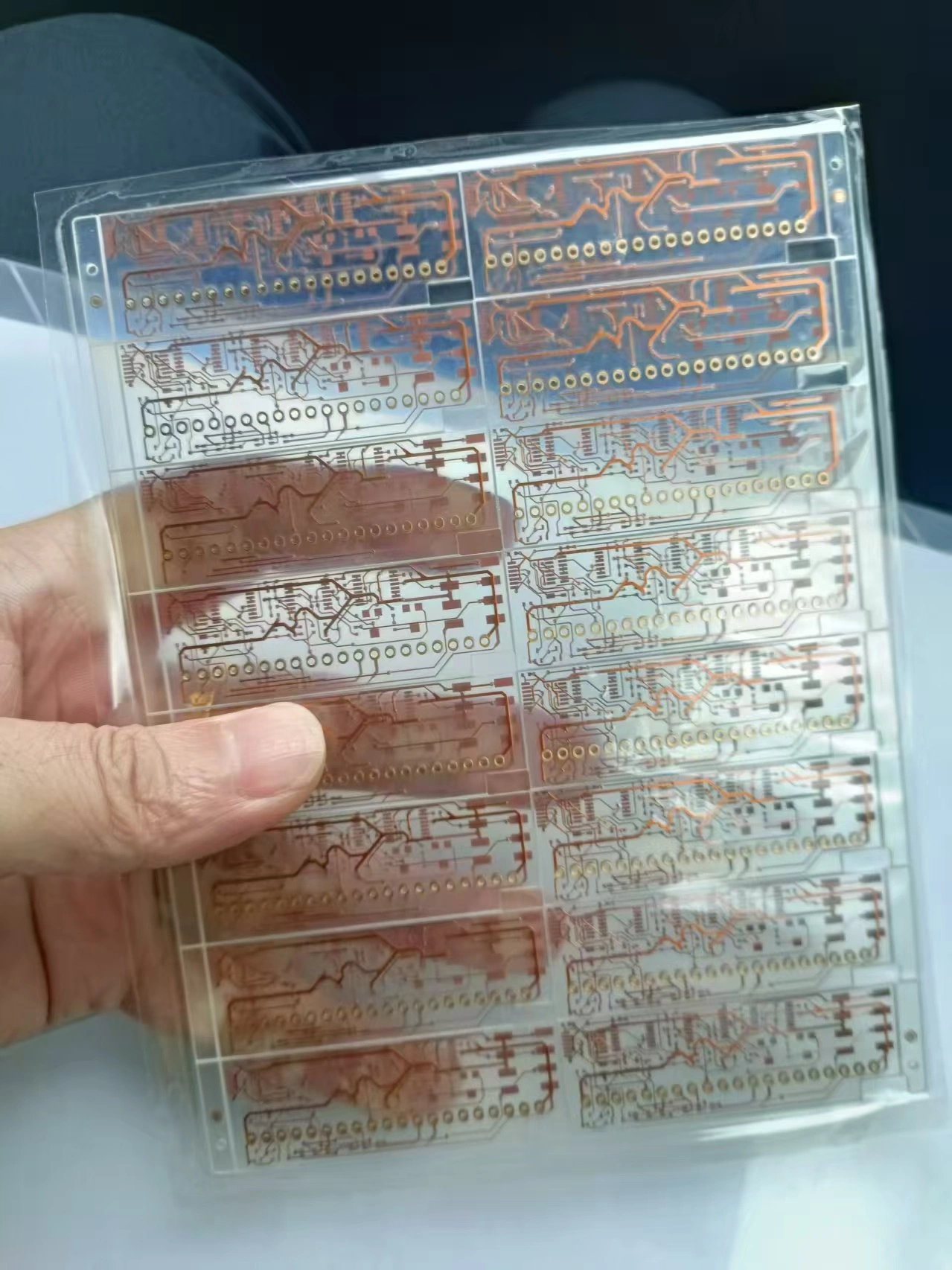
PET Transparent Single-layer Double-layer Flexible FPC,Single Layer PET Material Flexible Flexible Board FPC,pcb,fpc,pcba,SMT


Product Spotlights
Related Products
-
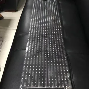
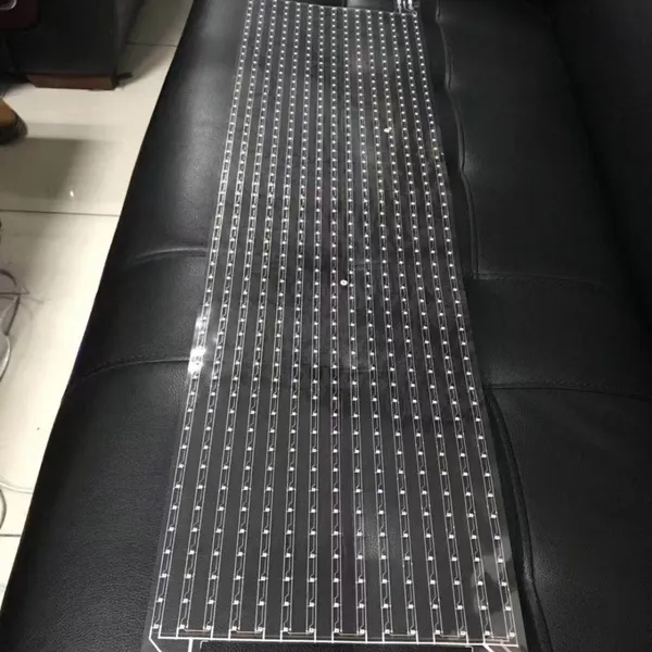
 2-layer PET Material Ultra Long Board FPCNegotiableMOQ: 1 Blade
 -
2-layer Transparent FR-4 Material Ultra Long Ultra-thin PCB,Ultra Thin Transparent FR-4PCBNegotiableMOQ: 1 Blade
-
Button Transparent PET Carbon Wire FPCNegotiableMOQ: 1 Blade
-
Film Switch Transparent PET Silver Wire FPCNegotiableMOQ: 1 Blade
-
1-6 Transparent FR-4 Circuit Board PCBNegotiableMOQ: 1 Blade
If you have any needs, please feel free to contact China Chaosheng Electronics Company. Please contact us as follows:
whatsapp:+8613528819118
Skype live: pcb-fpcb88@163.com
E-mail : sales@chaoshengpcb-fpc.com
Contact: Mank. Li
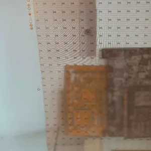
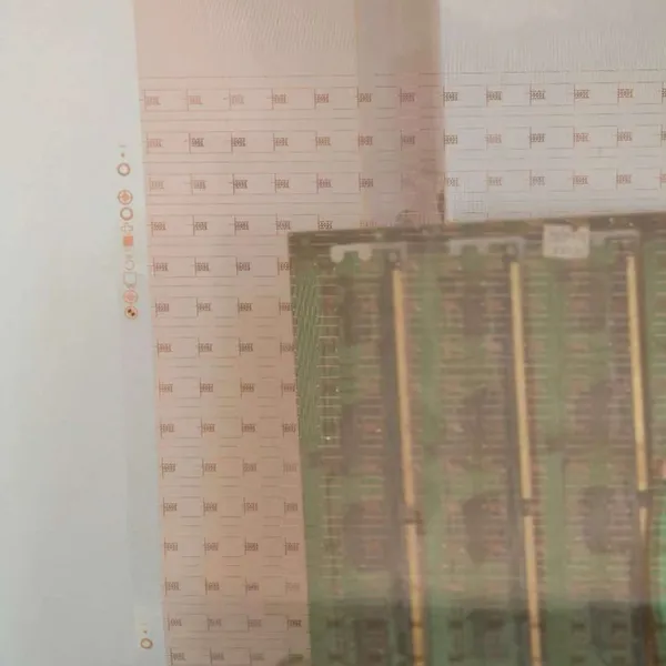
Product Name: LED, Display Screen
Board: PET
Layers: PET transparent single layer double layer flexible FPC
Minimum line width/spacing: 6/6mil
Finished product size: 250x1200mm/1 * 1PCS
Surface technology: OSP
Copper thickness: 35um
Plate thickness: 0.15mm
Minimum hole: 0.35mm
Features: Transparency meets 85-95% and can withstand normal temperatures of 220-240 degrees Celsius
Usage: Large size, LED transparent screen, display frequency, LED glass screen, etc
Main Product Structure of Chaosheng Group Company
Transparent PETFPC,Transparent FR-4PCB,Ultra thin transparent FR-4PCB,Transparent PCB display screen,Transparent FR-4PCB display screen,LED transparent screen PCB,Button transparent PET carbon wire FPC,Film switch transparent PET silver wire FPC,Thin film switch FPC,Thin film switch carbon wire FPC,Thin film switch silver wire FPC,Transparent Screen Transparent PCB,Transparent glass PCB,Glass screen PCB,Tempered glass PCB
2-80 layers of rigid circuit boards, 2-50 layers of flexible circuit boards and PCBA production
Chaosheng Group Company mainly produces product categories
High end double-sided, multi-layer, flexible, high-frequency, HDI interconnect, metal based, high thermal conductivity metal based, ceramic, cut in metal based, cut in buried capacitor, cut in thick copper buried magnet, concave convex step substrate, 5G high-speed board, thick copper, thick gold, high carbon resistance, double-sided multi-layer MiNiLED, MiNiHDILED, MiNiOLED, IC carrier substrate, roll to roll FPC, long FPC, large-sized printed circuit board, halogen-free material, high-frequency material, high-speed material, metal material, environmentally friendly circuit board, blind buried hole circuit board, high thermal conductivity aluminum based, thermoelectric separation copper based, PDU busbar, iron-based and metal based (core) mixed pressure plate, embedded copper buried copper. Buried resistance buried capacitance buried ceramic bead board, ultra-thin BT board, ceramic substrate, IC carrier board, high-frequency mixed voltage, high-speed board, differential impedance board, thick copper plate, thick gold plated board, HDI An integrated OEM and ODM production factory for Anylayer, double-sided, multi-layer, HDI FPC, soft hard combination HDI, roll to roll FPC, ultra long FPC, ultra large size PCB production and product design and development, software development, special material printed circuit boards, etc.
The main application areas of PCB and PCBA products of Chaosheng Group Company
Communication terminals, communication stations, electronic communication, fiber optics, optical modules, backlight sources, chip systems, communication equipment, communication instruments, computers, intelligent devices, intelligent control, system control, industrial power control, industrial equipment, testing instruments, testing instruments, SD cards, SG cards, mobile phones, computers, various antennas, radars, automobiles, light sources, resistors, music equipment, playback equipment, banking equipment, medical instruments, medical equipment, aerospace, aviation, military, LED, OLED, OLCD power control power supply, industrial power supply, communication power supply, automotive power supply, office equipment, digital products, computers and other application fields;
The main application areas of flexible circuit boards (FPC) and FPCA products of Chaosheng Group Company
Hard drives, printers, fax machines, scanners, sensors, mobile phones, connectors, modules, walkie talkie antenna cards, high-end cameras, digital cameras, laser heads, CDs, medical devices, instruments, drives, automobiles, automotive instruments, automotive drive disks, drivers, optical drives, medical devices, medical equipment, backlight sources, modules, banking equipment, industrial instruments, LED light strips, military, aviation, aerospace, national defense and other product fields.
|
Process Capability Table | ||||
| Technical ltem | MassProduct | Advanced Technology | ||
| 2015 | 2021 | 2025 | ||
| PMax.Layer Count | 80 layer | 100 layer | 100 layer | |
|
PCB through hole board |
2~80 layer | 2~100 layer | 2~100 layer | |
|
Maximum size through hole 1~2 |
37〞*98.50" | 43.3〞*118.11" | 43.3〞*118.11" | |
|
Minimum line width and spacing |
10(0.40) | 10(0.40) | 7.50(0.30mm) | |
| Minimum mechanical hole(mm) |
12(0.50) | 10(0.40) | 8.50(0.35mm) | |
|
Maximum size through hole 4~22 layers |
37〞*43.30" | 43.3〞*43.30" | 43.3〞*43.30" | |
|
Maximum size through hole 4~22 layers |
31.50 ″*59" | 31.50 ″*70.86" | 31.50 ″*70.86" | |
|
Maximum size through hole 4~22 layers |
10(0.40) | 10(0.40) | 7.50(0.30mm) | |
|
Minimum line width and spacing for multi-layer large-sized PCBs |
10(0.40) | 10(0.40) | 7.50(0.30mm) | |
|
Maximum size of multi-layer through- hole : 4-22 layers with the smallest hole |
12(0.50) | 10(0.40) | 8.50(0.35mm) | |
|
Maximum size HDI 4~36 layers |
31.50 ″*55" | 31.50 ″*55" | 31.50 ″*55" | |
|
Minimum line width and line spacing of large size PCB |
Through hole 12 / 12milHDI14 /14mil |
Through hole 10/10 milHDI12 / 12mil |
Through hole 8 / 8milHDI12 / 12mil |
|
|
The largest board ruler 1 → the smallest hole of 18 layers |
Through hole 0.50mmHDI :0.45mm |
Through hole 0.50mm HDI : 0.45mm |
Through hole 0.50mmHDI : 0.45mm |
|
| The layer number of FPC | 1~36layer | 1~60layer | 1~60layer | |
| Maximum size of flexible FPC |
19.68〞*55" | 28〞*59" | 31.49〞*118.12" | |
| Maximum size of flexible FPC with soft hard combination |
19.68〞*55" | 28〞*59" | 31.49〞*118.12" | |
|
FPC (roll to roll) maximum size |
19.68 ″*7874" | 19.68 ″*7874" | 19.68 ″*7874" | |
|
Maximum size of FPC single chip shipment |
19.68 ″*118.11" | 19.68 ″*196.8" | 19.68 ″*196.80" | |
| The layer number of FPC | 2~18 layer | 2~36 layer | 2~42 layer | |
|
Maximum size of layered board |
19.68 ″*35" | 19.68 ″*43" | 19.68 ″*43" | |
|
Number of through-hole layers |
2~20layer | 2~30 layer | 2~40 layer | |
|
Hard and soft HDI layers |
2~14 layer | 2~18 layer | 2~22 layer | |
|
Maximum size of soft and hard combination |
19.68 ″*43" | 19.68 ″*49" | 19.68 ″*49" | |
|
FPC/soft-hard combination arbitrary interconnection HDI |
4+X+4Interconnect HDI |
5+X+5Interconnect HDI | 6+X+6Interconnect HDI |
|
|
HDIPCB layers |
4~36layer | 4~60layer | 4~80 layer | |
|
Anylayer HDI PCB |
4+X+4Interconnect HDI |
5+X+5、Interconnect HDI | 8+X+8、Interconnect HDI |
|
|
HDIPCB maximum board size |
24"*52" | 43"*49" | 43"*49" | |
|
Number of through hole layers of high frequency board |
2~18 layer | 2~36 layer | 2~60 layer | |
| HDI layers ofhighfrequency board |
2~16 layer | 2~24 layer | 2~60layer | |
| Maximum size of high frequency board |
37 ″*43" | 43 ″*49" | 43 ″*49" | |
|
Number of ceramic plates |
1-2 layer | 1~4 layer | 1~6 layer | |
|
Ceramic plate thickness |
0.60mm-1.60mm | 0.38mm-20.0mm | 0.38mm-20.0mm | |
|
Maximum size of ceramic plate |
100*150mm | 150*190mm | 150*650mm | |
Serial Number Project Manufacturing capability
1 Layers Floors 1-80
2 Maximum size of PCB 2500*1150mm
3 Maximum size of flexible FPC 500mm*100m
4 Maximum size of PCBA 1600mm*1000mm
5 FPCBA maximum size 500mm*100m
6 PCB finished product thickness 0.15-12.0mm
7 Thickness of flexible FPC finished product 0.05-0.60mm
8 Finished copper thickness 12um-1075um
9 Minimum finished aperture of laser hole 0.075mm
10 Minimum line width and spacing 1.5mi/1.50mil
11 Minimum finished hole diameter for through-hole 0.15mm
12 Thickness stacking aspect ratio 1:35
13 By processing methods VIA blind buried hole treatment: ink plug hole, resin plug hole, copper paste plug hole, VCP copper filling hole, silver paste plug hole, carbon oil plug hole, etc
14 Surface Treatment Sinking gold, electroplating nickel gold, electroplating thick gold, electroplating gold+OSP, electroplating nickel gold+sinking gold, electroplating nickel gold+sinking gold+OSP, electroplating gold+OSP, electroplating gold+gold fingers, OSP+gold fingers, lead-free tin spraying, lead-free tin spraying+sinking gold, lead-free tin spraying+gold fingers, lead tin spraying, OSP, sinking tin, sinking silver, electroplating silver
15 Main substrate brands Rogers, Arlon, Taconic, TP-2, Megtron, Neclo, Isola, F4B, 3M, Mitsui Group (Japan Mitsui/Mitsui Top), Taiyo TUC, Taiguang EMC, Tenghui VT, Shengyi SY, Lianmao ITEQ, South Asia NOUYA, DuPont Kappon, Taihong, Hongren Hongren, Xin Yang, Nippon Steel Nippon Stee, Teflon, Yasen, Matsushita, RCC, Mitsui Mitsui Group (Japan Mitsui Top), 3M (USA) 3M Location, Kyocera CERADIR, Jiuhe, Jiuhao, China Porcelain, Huaqing, Ai Shengda, Slitton, Kai Changde, Tongxin, Bergs, Yalong, Taiconieta, etc
16 Solder mask color Green, black, red, yellow, white, blue, purple, matte green, matte black, etc
17 Test service AOI、X-Ray、 Voltage withstand test, short circuit test, soldering test, thermal shock test, functional test, high temperature and high humidity test, first piece tester, etc
18 Molding method CNC shape, punch shape, V-CUT+forming method
19 Finished product warpage ≤0.5%
20 Mechanical aperture tolerance ≤0.025mm
21 Finished product warpage ≤0.5%
22 MiNiLED Minimum PAD 0.065mm/0.065mm
23 Thermal conductivity ≧8W
24 Highest withstand voltage 2500Pa
25 High carbon resistance value and tolerance ≧100→15000Ω±20%
26 Impedance tolerance ≤5→8%Ω
27 IC Carrier Board Series Minimum line width and spacing of 20um/20um
FAQ
Question Point Answer
Q: What information is required for PCB CEGSATE: Gberber files for PCB production, product process instructions, such as material requirements, surface treatment requirements, finished product thickness requirements, PCB stack structure diagram for advanced products, copper thickness requirements for each layer, sample quantity requirements, batch order requirements, product application fields, and other related information are required
Q: What information does PCBA need to provide CEGSATE: BOM report is required (including the brand, specifications, and model of the components), X and Y coordinate numbers of PCBA components, and processing requirements: Do we need to purchase the components on our behalf? Or customer supplied components? Do you need software burning? What is the required quantity? What is the monthly demand and other detailed information.
Question: Is my file secure? CEGSATE: Your files are very secure, and we protect intellectual property rights for our clients throughout the entire process. All files provided by the customer will never be shared with any third party.
Q: What is the minimum order quantity? CESGATE: There is no minimum order quantity in POE. We are able to handle small and large batches flexibly.
Q: Do you have any other services? CESGATE: We mainly focus on PCB+FPC production+SMT+assembly PCBA+component procurement services; In addition, we can also provide programming, testing, software burning, wiring, and shell assembly services; And product design, product development, software development
Q: What is your inspection method? How do you control the quality? CESGATE: In order to ensure the quality of PCB and FPC products, flying pin testing is usually used for samples and small batches; The inner circuit undergoes AOI optical inspection, online AOI inspection, and the finished product undergoes 100% inspection through E-SET testing rack. The appearance undergoes 100% inspection through fully automatic finished product inspection equipment and FQC. PCBA undergoes automatic optical inspection (AOI), BGA part X-Ray 100% radiographic inspection, and first article inspection (FAI). PCBA products that require software burning undergo 100% full testing through finished product testing rack according to product functional requirements.

Send Inquiry to This Supplier


You May Also Like
-
6 Transparent FR-4 Circuit Boards PCBNegotiableMOQ: 1 Blade
-
Transparent Glass Circuit Board PCB, Copper Wiring Transparent Glass PCBNegotiableMOQ: 1 Blade
-
Transparent Tempered Glass Circuit Board PCB, Copper WiringNegotiableMOQ: 1 Blade
-
Tempered Glass PCB Glass PCBNegotiableMOQ: 1 Blade
-
China Chaosheng Electronics, Fake Double-layer Perforated Flexible FPC, Model CSFPC23650, Ultra-thin, FlexibleNegotiableMOQ: 1 Blade
-
China Super Sheng Twelve Layer HDI Soft Hard Combined FPC, DuPont Material, LCD Display Motherboard Flexible FPCNegotiableMOQ: 1 Blade
-
China Super Sheng 12 Layer Arbitrary Order HDI Soft Hard Combination FPC, Laptop Motherboard Circuit Board Layout Flexible Circuit BoardNegotiableMOQ: 1 Blade
-
Chaosheng Electronics, Ultra Long Flexible FPC, TAB Products and LED, Tape and Roll to Roll Flexible Circuit Boards, Strip Ultra Long Flexible BoardsNegotiableMOQ: 10 Blades
-
Double Layer Transparent FR-4PCB,Multi Layer FR-4 Transparent PCB,Is the Cost of Producing Multi-layer Transparent CircuitNegotiableMOQ: 1 Unit
-
Transparent FR-4PCB,FR-4, TG130 Material,PI Transparent Flexible Board FPC,Computer Keyboard Transparent FR-4 Transparent Material PCBNegotiableMOQ: 1 Unit


