








 Contact Platform Support
 Help Center
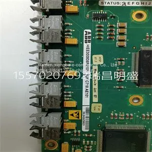
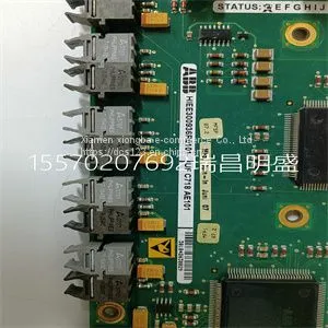
Module Spare Parts UFC718AE101 HIEE300936R0101



Related Products
-
 Module Spare Parts UFC721BE101 3BHE021889R0101US$ 1 - 100000MOQ: 1 Piece
 -
Module Spare Parts UFC760BE1142 3BHE0Q4573R1142US$ 1 - 100000MOQ: 1 Piece
-
Module Spare Parts UFC760BE43 3BHE004573R0043US$ 1 - 100000MOQ: 1 Piece
-
Module Spare Parts UFC762AE101 3BHE006412R0101US$ 1 - 100000MOQ: 1 Piece
-
Module Spare Parts ULTRA SLIMPAKG448-0002US$ 1 - 100000MOQ: 1 Piece
Focus on DCS, PLC, robot control system and large servo system.
Main products: various modules / cards, controllers, touch screens, servo drivers.
Advantages: supply of imported original products, professional production parts,
Fast delivery, accurate delivery time,
The main brands include ABB Bailey, Ge / fuanc, Foxboro, Invensys Triconex, Bently, A-B Rockwell, Emerson, ovation, Motorola, xyvom, Honeywell, Rexroth, KUKA, Ni, Deif, Yokogawa, Woodward, Ryan, Schneider, Yaskawa, Moog, prosoft and other brands
| UFC718AE101 HIEE300936R0101 |
7.3 Feature Description 7.3.1 Overvoltage Protection The LM3481 has overvoltage protection (OVP) for the output voltage. OVP is sensed at the feedback pin (FB). If at anytime the voltage at the feedback pin rises to VFB + VOVP, OVP is triggered. See the Electrical Characteristics section for limits on VFB and VOVP. OVP will cause the drive pin (DR) to go low, forcing the power MOSFET off. With the MOSFET off, the output voltage will drop. The LM3481 will begin switching again when the feedback voltage reaches VFB + (VOVP - VOVP(HYS)). See the Electrical Characteristics section for limits on VOVP(HYS). The Error Amplifier is operationnal during OVP events. 7.3.2 Bias Voltage The internal bias of the LM3481 comes from either the internal bias voltage generator as shown in the block diagram or directly from the voltage at the VIN pin. At input voltages lower than 6 V the internal IC bias is the input voltage and at voltages above 6 V the internal bias voltage generator of the LM3481 provides the bias. The voltage for the gate driver is output on the VCC pin for compensation by an external capacitor (0.47µF to 4.7µF depending on the FET requirements). Biasing the VCC pin by an external voltage source should not be attempted. + _ PWM Comparator Control Signal -M2 DTS (1-D)TS M1 MC = 0 Steady State Signal Vsamp Perturbed Signal 'Vsamp1 'Vsamp0 0.5, ΔVsamp1 will be greater than ΔVsamp0. In other words, the disturbance is divergent. So a very small perturbation in the load will cause the disturbance to increase. To ensure that the perturbed signal converges we must maintain:

Send Inquiry to This Supplier


You May Also Like
-
Module Spare Parts UNS4881b,V4 3BHE009949R0004US$ 1 - 100000MOQ: 1 Piece
-
Module Spare Parts UR6AHUS$ 1 - 100000MOQ: 1 Piece
-
Module Spare Parts VT-HNC100-1-23W-08-P-0 R900958999US$ 1 - 100000MOQ: 1 Piece
-
Module Spare Parts07AC91 GJR5252300R0101US$ 1 - 100000MOQ: 1 Piece
-
Module Spare Parts 07DC91C GJR5251400R0202US$ 1 - 100000MOQ: 1 Piece
-
Module Spare Parts 07EA90-SI GJR5251200R0101US$ 1 - 100000MOQ: 1 Piece
-
Module Spare Parts 07KR51 1SBP260011R1001US$ 1 - 100000MOQ: 1 Piece
-
Module Spare Parts 07KT98 GJR5253100R3160US$ 1 - 100000MOQ: 1 Piece
-
Module Spare Parts 086318-002 086318-501US$ 1 - 100000MOQ: 1 Piece
-
Module Spare Parts 086339-001 004707001474US$ 1 - 100000MOQ: 1 Piece


