

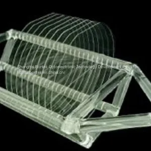
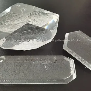
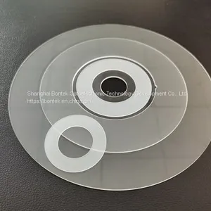
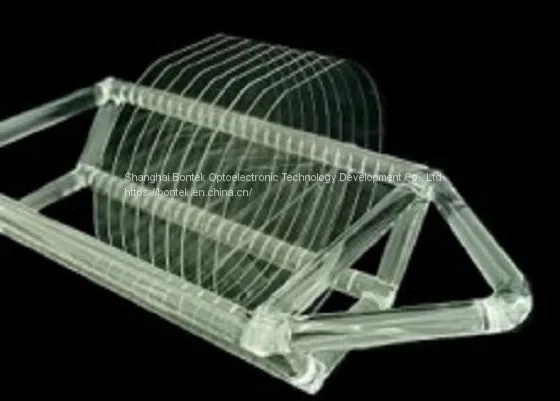
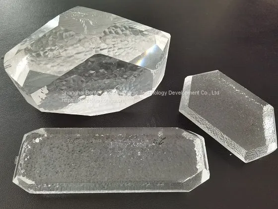
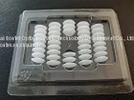
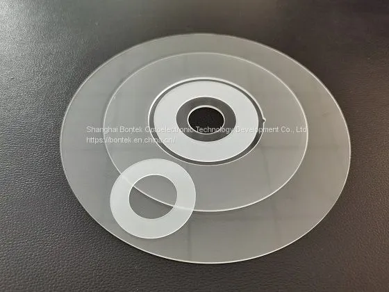
Quartz Crystal Wafers/Rings/Blanks

Related Products
Single crystal quartz wafers/blanks are made of synthetic quartz crystal. It has good piezoelectric effect and is widely used in timing frequency control, frequency selection and QMEMS. Cutting-edge applications include VCXO, TCXO, OCXO etc.
Material Characteristics
Material |
Piezo / Optical grade |
Q-Value |
Min 1.8x10^6, 2.4x10^6 to 3.0x10^6 IEC standards |
ECD |
Max 2 /c㎡, 10/c㎡, Max 30/c㎡, Max 100/c㎡, Max 300/c㎡; Swept Quartz |
Inclusions Density |
Ia, Ib, I, II, III Grades |
Swept |
Both Pure Z and Y Bar available,with or without Swept quartz |
processing capacity - blanks
Cuts Type (orientation) |
X, Y, Z, AT, BT, CT, ET ,DT, GT, NT, FC, SC, IT, AC, BC, ST, TS MT ,NT RT, LC…, etc |
Angle Tolerance(±) |
Theta Angle: ±5″, ±10″, ±15″, ±30″, ±1′, ±2′, …, etc. |
Phi Angle: ±5′, ±10′, ±15′, ±30′, …, etc. | |
Size |
Round (3.0mm~8”)/ Square (1.6x1.6mm~48x48mm or larger)/ SMD (1.2x2.4mm Above) |
Size Tolerance(±) |
±0.01mm,+/-0.005mm, +/-0.0005mm, according to size |
Frequency/ Thickness |
1 Mhz up to 54Mhz for AT-Cut Fundamental; Up to 70Mhz by Etching |
Flat |
Per requested: the flat shall be perpendicular to X axis within ±10 deg |
Surface Finishing |
#1000(9u); #2000(7u); #3000(5u); #4000(3u) (Sic); Polished(Cerium oxide)& etched Std |
Overtone |
Fundamental; Third Overtone (3rd); Fifth Overtone (5th) |
Contouring (dioptric) |
Plano-Convex : 0.5 dioptric~10 dioptric Bi-Convex: 10 dioptric~15 dioptric |
processing capacity - wafers
Diameter |
3”(76.2mm) |
4”(100mm) |
6”(150mm) |
8”(200mm) |
Thickness |
0.08mm Min-up |
0.10mm Min-up |
0.20mm Min -up |
0.35mm Min- |
Primary Flat |
22mm |
32mm |
42.5mm |
57.5mm or notch |
Surface |
LTV (5mmx5mm) |
TTV |
||
Bow |
-30 |
Warp |
||
Surface Type |
SSP / DSP |
Edge Criteria |
R=0.2mm or Bullnose |
|
Polished side Ra |
Back Side Criteria |
General is 0.2-0.5µm or as customized |

Send Inquiry to This Supplier


You May Also Like
-
 ATEX Certified KL1.2Ex Cordless LED Miner Cap Lamp Explosion Proof Mining HeadlampUS$ 75 - 85MOQ: 1 Piece
 -
QuartzNegotiableMOQ: 2500 Tons
-
Little Diamond Quartz Heater/Quartz Tube Heating(Wechat:13510231336)NegotiableMOQ: 2000 Pieces
-
Quartz Sand Drying Plant ManufacturerNegotiableMOQ: 1 Set
-
High Temperature Round Quartz Boiler Sight Glass ProductionNegotiableMOQ: 100 Pieces
-
Heart Shaped Pink Quartz Gua ShaNegotiableMOQ: 1
-
3R Raymond Stone Grinding Mill Machine for Limestone Calcite Quartz Powder MakingUS$ 3200MOQ: 1 Set
-
Industrial Rotary Quartz Sand Slag Clay Gypsum Sawdust Coal Block Sludge Drum Dryer EPCUS$ 9500 - 9800MOQ: 1 Combo
-
High Quality Quartz Sand Filter Water Treatment Machinery Stainless Steel Filter Carbon Steel Sand FilterUS$ 2630 - 2650MOQ: 1 Piece
-
Genyond Apm Mineral Color Sorting Machine China Ore Sorting System Quartz Powder Optical Sorter on Mineral PlantUS$ 39900.00MOQ: 1 Set


