

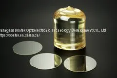
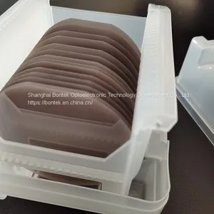
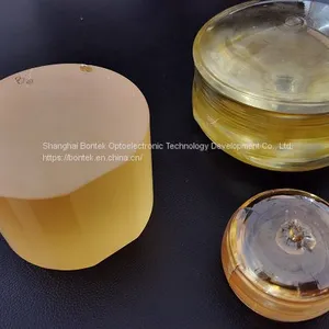
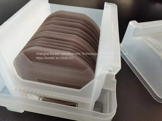
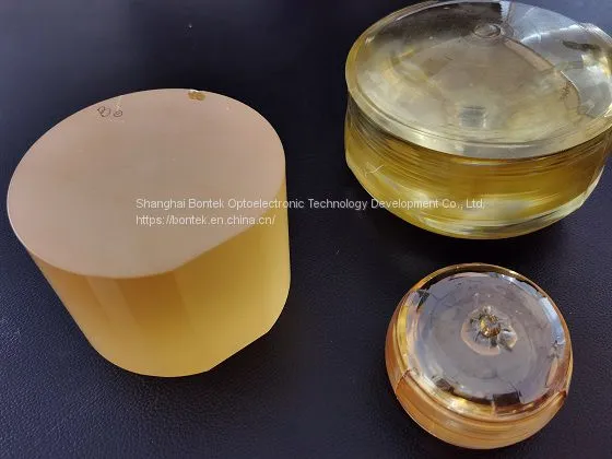
Lithium Niobate Wafer

Related Products
-
 Lithium Tantalate WaferNegotiableMOQ: 5 Pieces
 -
Quartz Crystal Wafers/Rings/BlanksNegotiableMOQ: 5 Pieces
-
Fused Silica/Quartz WaferNegotiableMOQ: 5 Pieces
-
Fluoride Optical Window/Prism/LensNegotiableMOQ: 5 Pieces
-
Lithium Niobate LN Wafers for Photonics and OptoelectronicsNegotiableMOQ: 25 Pieces
Lithium Niobate has good nonlinear optical properties and can be used as optical waveguide material, or to produce medium and low frequency SAW filter, high power high temperature resistant ultrasonic transducer, etc. Lithium niobate doping is now widely used, such as Mg:LN, Nd:Mg:LN, Fe:LN.
Material Characteristics
Material |
3" 4" 6" 8" LN wafer Saw/Optical grade |
Orientation |
X/Z/Y41°/Y64°/Y128°/YZ/YX or Customized |
Curie Temp |
1142°C±3°C |
Doped with |
Zn, MgO single or double doped available |
processing capacity
Surface finish |
single or double sides polish (DLP/SLP/ SSP/DSP all available ) |
|
Thickness |
0.18/0.25/0.35/0.50/1.00 mm |
0.25/0.35/0.50/1.00 mm |
TTV |
||
BOW |
± (25µm ~40um ) |
|
Warp |
||
LTV (5mmx5mm) |
||
PLTV( |
≥98% (5mm*5mm) with 2mm edge excluded |
|
Edge |
Compl't with SEMI M1.2 with GC800# .regular at C typed |
|
Orientation flats |
available, per request |
|
Polished side Ra |
Roughness Ra |
|
Back Side Criteria |
Roughness Ra:0.5-1.0µm GC#1000 |
|
Edge Rounding |
Compliant with SEMI M1.2 Standard/refer to IEC62276 |
|
Cracks, saw marks, stains |
None |
|

Send Inquiry to This Supplier


You May Also Like
-
Lithium Niobate WaferNegotiableMOQ: 5 Pieces
-
New Design 5 in 1 Optical New Energy Fiber Laser Welding Machine for Lithium Battery Copper AluminumNegotiableMOQ: 1 Set
-
Double Laser Orthogonal Optical Bench Wet Mode Winner2005A Lithium Manganese Oxide Particle Size Analysis Testing MachineUS$ 1 - 2MOQ: 1 Set
-
3.6V Optical Cordless Screwdriver With Lithium BatteryUS$ 8 - 9MOQ: 500 Pieces
-
Lithium Fluoride Raw Block, Optical Crystal GlassesUS$ 5.01 - 20MOQ: 1 Piece
-
Built-in Battery Rechargeable Lithium Battery Optical Bluetooth Wireless MouseUS$ 1 - 8MOQ: 50 Pieces
-
15Mp Max Resolution 4X Optical Zoom Digital Camera Lithium BatteryUS$ 1 - 50MOQ: 500 Pieces
-
Optical Fiber Fusion Splicer Lithium Battery Manufacturer With CE,ROHS,UL CertificatesNegotiableMOQ: 100 Packs
-
NFION NF150-500N Thermal Conductive Gel for Photovoltaic and Optical Modules Thermal Conductive Gel for New Energy Lithium Batteries Silica GelUS$ 0.1 - 10MOQ: 100 Pieces
-
Cheap 18MP Max 6X Optical Zoom 1080P Full HD Video Digital Camera Still Image Photo Camera 2.4" Color Screen Lithium BatteryUS$ 15 - 25MOQ: 10 Pieces


