








 Contact Platform Support
 Help Center
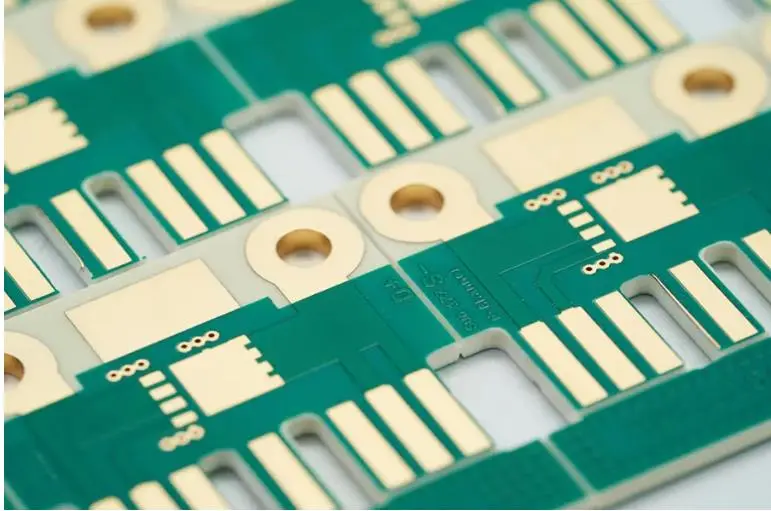
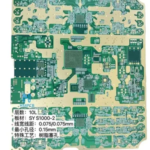
Multi‑layer HDI Blind‑Buried Via PCB for 800G Transceiver,China Chaosheng Electronics | 800G Communication Multilayer High Speed High Frequency PCB
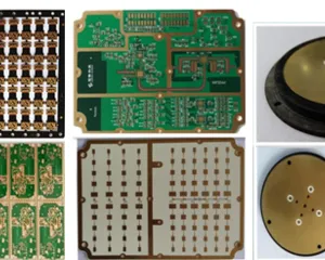
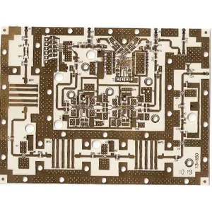
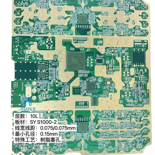
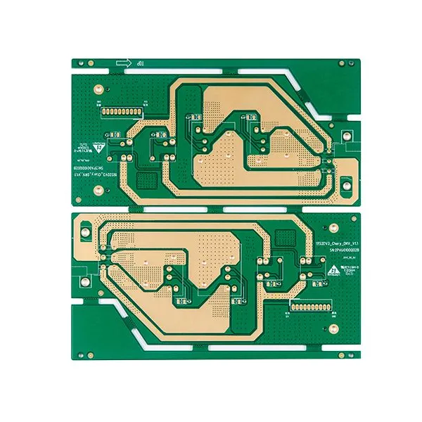
Product Spotlights


Related Products
-
 China Chaosheng Electronic Aviation Products High Frequency High Speed Multilayer Circuit Board PCBNegotiableMOQ: 20 Blades
 -
China Chaosheng Electronic Radar Products High Frequency High Speed Multilayer Circuit Board PCBNegotiableMOQ: 1 Blade
-
China Chaosheng Electronics' Frequency Closed Products Include High-frequency and High-speed Multi-layer Circuit Boards (PCBs)NegotiableMOQ: 1 Blade
-
China Chaosheng Electronics 800G Optical Communication, Optical Module High-frequency High-speed Multi-layer Circuit Board PCBNegotiableMOQ: 1 Blade
-
12 Layers, 2nd Order High-frequency Mixed Voltage, 2nd Step PCBNegotiableMOQ: 20 Units
If you have any needs, please feel free to contact China Chaosheng Electronics Company. Please contact us as follows:
whatsapp:+8613528819118
Skype live: pcb-fpcb88@163.com
E-mail : sales@chaoshengpcb-fpc.com
Contact: Mank. Li
China Chaosheng Electronics | 800G Communication Multilayer High Speed High Frequency PCB Complete Product Technical Solution
Compatible with QSFP-DD, OSFP, 800G optical modules, AI computing power switch motherboards, CPO co packaged optical boards, high-speed backboards, soft and hard combination FPC cables, fully covering substrates, precision processes, signal control, surface technology, supporting FPC flexible interconnection, and one-stop processing of thin film silver wire touch panels.
1、 Core substrate selection (800G-PAM4 single channel 112Gbps transmission standard)
All use ultra-low loss high-speed boards to avoid the high insertion loss defect of ordinary FR-4 high-frequency plugs
1. * * Panasonic Megtro-7 * *: Dk=3.3, Df ≤ 0.0013@10GHz The main 800G optical module substrate has extremely low dielectric loss and stable impedance
2. Rogers RO4350B, PTFE ceramic composite high-frequency sheet, used for ultra-high frequency links above 56GHz
3. Isola MT77、 Taiguang IT-988GSE high-speed board, specialized material for multi-layer motherboards of switches
4. High frequency mixed compression process * *: Ultra low loss board is used for the high-speed signal layer, and modified FR-4 is used for the power layer. The cold and hot cycles are 50000 times without delamination, reducing production costs by 22% and reducing insertion loss by 18% at 28GHz
Rigid electrical indicators of sheet metal
-Working bandwidth: 0-56GHz, compatible with PAM-4 modulation signals
-28GHz wiring insertion loss ≤ 2dB/inch
-Wide temperature range -40 ℃~125 ℃, dielectric constant fluctuation ≤± 0.02, eliminating impedance drift
2、 Multilayer board stacking and specification parameters
1. Can produce * * 6-32 layers of high-order HDI high-frequency PCB * *; The 800G optical module comes standard with 8-12 layers of third-order blind buried hole structure, and the switch backplane has a maximum of 30 layers or more
2. Finished board thickness: 0.4mm-3.2mm; Thin layer lamination of ultra-thin core board 0.08mm
3. The maximum thickness to diameter ratio is 8:1, and the current carrying capacity of high-power optical module power via holes is sufficient
4. The differential impedance tolerance is strictly controlled within ± 5% (conventional FR-4 can only achieve ± 10%), and the TDR time-domain reflectometer is used for full board impedance detection
3、 Core process of precision manufacturing
1. HDI laser micro hole process
-The minimum aperture of UV laser blind hole is 75 μ m, and the hole position accuracy is ± 5 μ m
-BGA solder pads are directly laser fanned out, with a solder pad ring width of ≥ 3mil, to prevent breakage and open circuits; The wiring density can reach 200 points/cm ², suitable for OSFP compact packaging
-Buried hole, first-order to fourth-order blind buried hole process, shortening high-speed signal path and reducing signal jitter
2. Ultra fine line etching
1. Laser direct imaging LDI, minimum line width/spacing 25 μ m-30 μ m
2. Low roughness and ultra-low profile copper foil, reducing high-frequency skin loss
3. Differential control of internal length error
3. Compression, heat dissipation and stability process
1. CNC constant temperature lamination, temperature field accuracy ± 1 ℃, interlayer alignment deviation of multi-layer board ≤ 15 μ m
2. High frequency board dedicated plasma debonding process, uniform electroplating on the inner wall of micropores
3. Low CTE stacked design, matched with thermal expansion of optical module laser chips, zero failure of high and low temperature cycling solder joints
4. High end surface treatment process (standard for 800G)
1. ENEPIG nickel palladium gold: preferred process, bonding gold wire, chip mounting, long-term oxidation resistance
2. Thick gold fingers, heavy gold, and heavy tin are optional; High speed connector gold finger gold plating thickness ≥ 1.5 μ m
4、 Signal integrity&electromagnetic control special technology
1. Complete high-speed impedance simulation, differential coupling, and complete reference layer grounding design
2. Partition grounding isolation, partition wiring for light emission, reception, and driving power supply to reduce crosstalk
3. Embed resistors and capacitors with built-in passive components, compress board area, and shorten high-speed wiring
4. Whole board AI AOI optical inspection, short circuit and open circuit testing, impedance sampling, high-voltage insulation testing
5、 800G integrated product line (PCB+FPC+silver wire film assembly)
1. Ultra large flexible FPC ribbon cable * *: High speed flexible ribbon cable between 800G optical module and motherboard, ultra-fine silver plated gold fingers, resistant to bending more than 100000 times
2. Display screen silver paste silver wire, nano silver touch melt screen, industrial large-scale thin film switch; Can be used as an optical module debugging control panel assembly
3. SMT surface mount, COB chip bonding, DIP plug-in, PCBA whole board OEM, one-stop delivery of complete circuit boards for optical modules
6、 Product application areas
800G-1.6T QSFP-DD/OSFP optical module, AI server switching backplane, data center high-speed communication equipment, CPO co packaged optical substrate, vehicle mounted high-speed communication board, high-end industrial control motherboard
7、 Service advantages
Support high-frequency and high-speed PCB rapid prototyping, small and medium batch production, and large-scale production; Capable of outputting DFM high-frequency manufacturability analysis, stacking schemes, and impedance reports; A complete set of customized touch screens that can be synchronously matched with multi-layer hard boards, soft hard combination boards, ultra large flexible FPCs, and silver paste conductive film switches.

Send Inquiry to This Supplier


You May Also Like
-
16 Layers, 3rd Order High-frequency Mixed Voltage, 6 Step PCB,multi-layer High-frequency High-speed Material PCBNegotiableMOQ: 10 Units
-
8 Layers, 3rd Order HDI High-frequency Mixed Pressure Buried Copper PCB,8th Layer 3rd Order Optical Module Buried Resistance PCBNegotiableMOQ: 20 Units
-
8 Layers, 2nd Order HDI High-frequency Mixed Voltage Buried Resistance PCB,8-layer 2nd Order Optical Module Embedded Gold Finger PCBNegotiableMOQ: 20 Units
-
8 Layers, 3rd Order HDI High-frequency Mixed Pressure Buried Capacitive Gold Finger PCBNegotiableMOQ: 20 Units
-
8 Layers of HDI High-frequency Mixed Pressure Buried Capacitor+buried Copper Block+gold Finger PCBNegotiableMOQ: 20 Units
-
6-layer High-frequency Multi-layer PCB,Taiyao TU872 High Speed MaterialNegotiableMOQ: 20 Units
-
16 High-frequency Multi-layer PCB,16 Layer High-frequency Mixed Voltage PCB,single-layer High-speed Material PCBNegotiableMOQ: 20 Units
-
6-layer High-frequency Multi-layer PCBNegotiableMOQ: 20 Units
-
18 High-frequency Multi-layer HDI PCB High-frequency Hybrid HDIPCBNegotiableMOQ: 1 Blade
-
Antimony Blind Gong HDI Multi-layer PCB,HDI High-frequency High-speed Material PCBNegotiableMOQ: 1 Blade


