

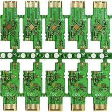
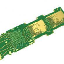
8 Layers, 2nd Order HDI High-frequency Mixed Voltage Buried Resistance PCB,8-layer 2nd Order Optical Module Embedded Gold Finger PCB

Related Products
-
 8 Layers, 3rd Order HDI High-frequency Mixed Pressure Buried Capacitive Gold Finger PCBNegotiableMOQ: 20 Units
 -
8 Layers of HDI High-frequency Mixed Pressure Buried Capacitor+buried Copper Block+gold Finger PCBNegotiableMOQ: 20 Units
-
6-layer High-frequency Multi-layer PCBNegotiableMOQ: 20 Units
-
16 High-frequency Multi-layer PCB,16 Layer High-frequency Mixed Voltage PCBNegotiableMOQ: 20 Units
-
6-layer High-frequency Multi-layer PCBNegotiableMOQ: 20 Units
Product areas: Communication equipment, optical communication
Layer number: 8 layers, 2nd order HDI high-frequency mixed voltage buried resistance PCB
Board thickness: 1.2mm
Size: 145 * 110mm/1 * 24 pieces
Process structure: Panasonic M7 high-speed material, inner and outer copper thickness of 1OZ, impedance ± 10%+buried resistance block PCB
Voltage withstand test: 100% short circuit test
The minimum mechanical hole is 0.15mm, and the laser hole is 0.075mm
Minimum line width and spacing of 3/4mil
Surface treatment: Nickel palladium 2U "+electric gold finger, gold thickness 20U", green solder mask
Features: Frequency closed signal interference, improved transmission speed, stable signal
Usage: Communication equipment, optical communication, instruments, meters, antennas, radars, aerospace, aviation, communication stations, 5G equipment, 5G communication, AI, Artificial intelligence, transmitters and other products
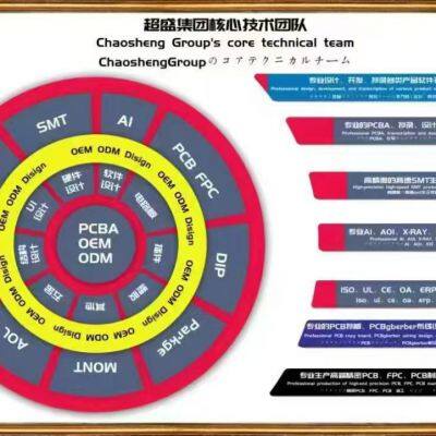
Main Product Structure of Chaosheng Group Company
2-80 layers of rigid circuit boards, 2-50 layers of flexible circuit boards and PCBA production
Chaosheng Group Company mainly produces product categories
High end double-sided, multi-layer, flexible, high-frequency, HDI interconnect, metal based, high thermal conductivity metal based, ceramic, cut in metal based, cut in buried capacitor, cut in thick copper buried magnet, concave convex step substrate, 5G high-speed board, thick copper, thick gold, high carbon resistance, double-sided multi-layer MiNiLED, MiNiHDILED, MiNiOLED, IC carrier substrate, roll to roll FPC, long FPC, large-sized printed circuit board, halogen-free material, high-frequency material, high-speed material, metal material, environmentally friendly circuit board, blind buried hole circuit board, high thermal conductivity aluminum based, thermoelectric separation copper based, PDU busbar, iron-based and metal based (core) mixed pressure plate, embedded copper buried copper. Buried resistance buried capacitance buried ceramic bead board, ultra-thin BT board, ceramic substrate, IC carrier board, high-frequency mixed voltage, high-speed board, differential impedance board, thick copper plate, thick gold plated board, HDI An integrated OEM and ODM production factory for Anylayer, double-sided, multi-layer, HDI FPC, soft hard combination HDI, roll to roll FPC, ultra long FPC, ultra large size PCB production and product design and development, software development, special material printed circuit boards, etc.
The main application areas of PCB and PCBA products of Chaosheng Group Company
Communication terminals, communication stations, electronic communication, fiber optics, optical modules, backlight sources, chip systems, communication equipment, communication instruments, computers, intelligent devices, intelligent control, system control, industrial power control, industrial equipment, testing instruments, testing instruments, SD cards, SG cards, mobile phones, computers, various antennas, radars, automobiles, light sources, resistors, music equipment, playback equipment, banking equipment, medical instruments, medical equipment, aerospace, aviation, military, LED, OLED, OLCD power control power supply, industrial power supply, communication power supply, automotive power supply, office equipment, digital products, computers and other application fields;
The main application areas of flexible circuit boards (FPC) and FPCA products of Chaosheng Group Company
Hard drives, printers, fax machines, scanners, sensors, mobile phones, connectors, modules, walkie talkie antenna cards, high-end cameras, digital cameras, laser heads, CDs, medical devices, instruments, drives, automobiles, automotive instruments, automotive drive disks, drivers, optical drives, medical devices, medical equipment, backlight sources, modules, banking equipment, industrial instruments, LED light strips, military, aviation, aerospace, national defense and other product fields.
| Process Capability Table | ||||
| Technical ltem | MassProduct | Advanced Technology | ||
| 2015 | 2021 | 2025 | ||
| Max.Layer Count | 80 layer | 100 layer | 100 layer | |
PCB through hole board | 2~80 layer | 2~100 layer | 2~100 layer | |
Maximum size through hole 1~2 | 37〞*98.50" | 43.3〞*118.11" | 43.3〞*118.11" | |
Minimum line width and spacing | 10(0.40) | 10(0.40) | 7.50(0.30mm) | |
| Minimum mechanical hole(mm) | 12(0.50) | 10(0.40) | 8.50(0.35mm) | |
Maximum size through hole 4~22 layers | 37〞*43.30" | 43.3〞*43.30" | 43.3〞*43.30" | |
Maximum size through hole 4~22 layers | 31.50 ″*59" | 31.50 ″*70.86" | 31.50 ″*70.86" | |
Maximum size through hole 4~22 layers | 10(0.40) | 10(0.40) | 7.50(0.30mm) | |
| Minimum line width and spacing for multi-layer large-sized PCBs | 10(0.40) | 10(0.40) | 7.50(0.30mm) | |
Maximum size of multi-layer through- hole : 4-22 layers with the smallest hole | 12(0.50) | 10(0.40) | 8.50(0.35mm) | |
| Maximum size HDI 4~36 layers | 31.50 ″*55" | 31.50 ″*55" | 31.50 ″*55" | |
| Minimum line width and line spacing of large size PCB | Through hole 12 / 12milHDI14 /14mil | Through hole 10/10 milHDI12 / 12mil | Through hole 8 / 8milHDI12 / 12mil | |
| The largest board ruler 1 → the smallest hole of 18 layers | Through hole 0.50mmHDI :0.45mm | Through hole 0.50mm HDI : 0.45mm | Through hole 0.50mmHDI : 0.45mm | |
| The layer number of FPC | 1~36layer | 1~60layer | 1~60layer | |
| Maximum size of flexible FPC | 19.68〞*55" | 28〞*59" | 31.49〞*118.12" | |
| Maximum size of flexible FPC with soft hard combination | 19.68〞*55" | 28〞*59" | 31.49〞*118.12" | |
FPC (roll to roll) maximum size | 19.68 ″*7874" | 19.68 ″*7874" | 19.68 ″*7874" | |
Maximum size of FPC single chip shipment | 19.68 ″*118.11" | 19.68 ″*196.8" | 19.68 ″*196.80" | |
| The layer number of FPC | 2~18 layer | 2~36 layer | 2~42 layer | |
Maximum size of layered board | 19.68 ″*35" | 19.68 ″*43" | 19.68 ″*43" | |
Number of through-hole layers | 2~20layer | 2~30 layer | 2~40 layer | |
Hard and soft HDI layers | 2~14 layer | 2~18 layer | 2~22 layer | |
Maximum size of soft and hard combination | 19.68 ″*43" | 19.68 ″*49" | 19.68 ″*49" | |
FPC/soft-hard combination arbitrary interconnection HDI | 4+X+4Interconnect HDI | 5+X+5Interconnect HDI | 6+X+6Interconnect HDI | |
HDIPCB layers | 4~36layer | 4~60layer | 4~80 layer | |
Anylayer HDI PCB | 4+X+4Interconnect HDI | 5+X+5、Interconnect HDI | 8+X+8、Interconnect HDI | |
HDIPCB maximum board size | 24"*52" | 43"*49" | 43"*49" | |
Number of through hole layers of high frequency board | 2~18 layer | 2~36 layer | 2~60 layer | |
| HDI layers ofhighfrequency board | 2~16 layer | 2~24 layer | 2~60layer | |
| Maximum size of high frequency board | 37 ″*43" | 43 ″*49" | 43 ″*49" | |
Number of ceramic plates | 1-2 layer | 1~4 layer | 1~6 layer | |
Ceramic plate thickness | 0.60mm-1.60mm | 0.38mm-20.0mm | 0.38mm-20.0mm | |
Maximum size of ceramic plate | 100*150mm | 150*190mm | 150*650mm | |
Minimum aperture of ceramic plate | 0.50mm | 0.35mm | 0.35mm | |
Minimum line width and line spacing of ceramic board | 16/16mil | 12/12mil | 10/10mil | |
Number of layers of metal copper substrate | 1-2 layer | 1~4 layer | 1~6 layer | |
Maximum line width and line spacing of metal iron substrate | 12/12mil | 4/4mil | 4/4mil | |
Number of layers of metal aluminum substrateHDI | 1-2 layer | 1~4 layer | 1~6 layer | |
Maximum size of metal substrate | 37 ″*43" | 25.59 ″*59" | 25.59 ″*59" | |
| The smallest hole of the metal substrate | 0.50mm | 0.35mm | 0.35mm | |
Minimum line width and line spacing of metal substrate | 8/8mil | 4/4mil | 4/4mil | |
| Transparent FR- 4 material layers | 1-2layer | 1-2layer | 1-8layer | |
| Transparent FR-4 minimum hole | 0.35mm | 0.35mm | 0.35mm | |
| Transparent FR-4 minimum line width and spacing | 4/4Mil | 4/4Mil | 3.5/3.5Mil | |
| Transparent FR- 4 maximum size | 23.63*47.25″ | 23.63*47.25 ″ | 23.63*47.25 ″ | |
| Number of tempered glass base layers | 1-2layer | 1-2layer | 1-2layer | |
| Minimum line width and spacing of glass | 4/4Mil | 4/4Mil | 3.5/3.5Mil | |
| The smallest hole in glass | 0.35mm | 0.35mm | 0.35mm | |
| Maximum size of glass | 23.63*47.25″ | 23.63*47.25 ″ | 23.63*47.25 ″ | |
| Number of layers of transparent PETmaterial | 1-2layer | 1-2layer | 1-2layer | |
| Maximum size of transparent PET | 19.68 ″*7874" | 19.68 ″*7874" | 19.68 ″*7874" | |
The company's main product types | Halogen free materials, high TG materials, high-frequency materials, high-speed materials, metal materials, glass materials, embedded materials, transparent FR- 4 materials, high thermal conductivity metals, high thermal conductivity aluminum substrates, environmentally friendly circuit boards, BT materials, ABF materials, and other imported materials, DU busbars, iron-based and metal based (core) mixed pressure plates, embedded buried copper, buried resistors, buried capacitors, buried ceramic bead plates, buried ceramics, ceramic mixed pressure plates, multi-layer ceramics, ultra-thin BT plates, ultra-thin PCBs, ultra-thin PCBs, multi-layer aluminum substrates, multi-layer ceramic plates, multi-layer ultra-thin HDI、 High frequency mixed voltage, differential impedance board, thick copper plate, gold-plated plate, high and low copper, high and low copper, high carbon resistance, transparent multilayer, glass plate, HDI arbitrary order (cross blind buried) Anylayer, flexible double-sided, flexible multilayer, soft hard combination HDI, roll to roll FPC, ultra long size, ultra large size board (single, double, multi-layer) PCB production and product design, product development, software development, etc | |||
| Main material | Rogers, Taikoni, Yaron, Mitsui, Isola, 3M, Taiyao, Taiguang, Tenghui, Shengyi,Lianmao, Nanya, Doosan, DuPont, Taihong, Hongren, Xinyang, Nippon Steel, Teflon,Yasen, Panasonic, RCC, Mitsui, Mitsubishi, Yingye, 3M, Kyocera, Jiuhao, Zhongci,Huaqing, Aishengda, Sliton, Kaichangde, Tongxin, Beige, Yalong, Taikoni,Hitachi, Laird System, etc | |||
Main material categories | Halogen-free、halogenated、 high thermal conductivity, high TG135 、TG140、 TG150、 TG170、TG180、TG240、TG320 | |||
| Build-up Material | FR-4 ,TG150,TG70,TG180 | |||
| Conventional plate thickness (mm) | Min.1-2L(mm) | 0.10mm | 0.10-12.0mm | 0.10-18.0mm |
| Min.4-10L(mm) | 0.35mm | 0.35mm~10.0mm | 0.35-18.0mm | |
| Min.12L(mm) | 0.43 | 0.38~10.0mm | 0.38~18.0mm | |
| Min.16L(mm) | 0.53 | 0.45~10.0mm | 0.45~18.0mm | |
| Min.18L(mm) | 0.63 | 0.51~10.0mm | 0.51~18.0mm | |
| Min.52L(mm) | 0.8 | 0.65~10.0mm | 0.65~18.0mm | |
| MAX(mm) | 3.5 | 12.0mm | 18.0mm | |
Copper plate thickness and copper thickness | 1-2 layerCU | 700um | 875um | 875um |
| Layers 4-20 | 4-12layer | 4-16layer | 4-22layer | |
| Inner layer copper thickness(um) | 875um | 1050um | 1225um | |
Outercopperthickness | 210um | 350um | 525um | |
Thick copper finished plate thickness | 8.0mm | 12.0mm | 18.0mm | |
| IC substrate | layerHDI | 1-10layer | 1-14layer | 1-16layer |
| Line width and spacing | 50um | 25um | 15um | |
| copper thickness | 8-10um | 10-12um | 12-15um | |
| Min.CoreThickness um(mil) | 254" (10.0) | 0.15~254(10.0mm) | 0.15~254(10.0mm) | |
| Min.Build up Dielectric | 38(1.5) | 25(1.0) | 25(1.0) | |
BaseCopperWeigh t | Inner Layer | 1/4-8 OZ | 1/4-0.30mm | 1/4-0.30mm |
| Out Layer | 1/4-10 OZ | 1/4-30 OZ | 1/4-30 OZ | |
| Gold thick | 1~40u" | 1~200u" | 1~200u" | |
| Nithick | 76~127u" | 1~250u" | 1~250u" | |
Min.HOle/Land um(mil) | 150/300(6/12) | 100/200(4/8) | 100/200(4/8) | |
Min.Laser via/landum(mil) | 60/170(2.4/6.8) | 50/150(2/6) | 50/150(2/6) | |
Min. IVH、Hole size/landum(mil) | 150/300(6/12) | 100/200(4/8) | 100/200(4/8) | |
| DieletricThickness | 38(1.5) | 32(1.3) | 32(1.3) | |
| 125(5) | 125(5) | 125(5) | ||
| SKipvia | Yes | Yes | Yes | |
| viaoNhie(laserviaon BuriedPTH) | Yes | Yes | Yes | |
| Laser Hole Filling | Yes | Yes | Yes | |
| Technicalltem | MassProduct | Advanced Technology | ||
| Hole depth/diameter | Through Hoie | 25:01 :00 | 35:01 :00 | 40:01 :00 |
| AspctRatio | MicroVia | 0.8 :1 | 0.8 :1 | 0.8 :1 |
| copperFilling Dimple Size | 10(0.40) | 5(0.20) | 5(0.20) | |
Minimumouter line width/ spacing | Inner layer line width and spacing | 38/38(1.5/1.5) | 38/38(1.5/1.5) | 38/38(1.5/1.5) |
PlatedLayerum(mil) | 38/38(1.5/1.5) | 38/38(1.5/1.5) | 38/38(1.5/1.5) | |
| BGAPitchmm(mil) | 0.4 | 0.4 | 0.4 | |
| PHMin.Hole rlng um(mil) | 75(3) | 62.50(2.50 | 62.50(2.50 | |
| Line Width control | <2.5mil(mil) | ±0.50 | ±0.50 | ±0.50 |
| 2.5mil≤L/W<4mil | ±0.50 | ±0.50 | ±0.50 | |
| ≤3mil(mil) | ±0.60 | ±0.60 | ±0.60 | |
| SolderMask Registration um(mil) | ±25 | ±25 | ±25 | |
| Solder masThickness | Lines Minum(mil) | 10(0.40) | 10(0.40) | 10(0.40) |
| Lines Minum(mil) | 30(1.20) | 30(1.20) | 30(1.20) | |
| CopperMinum(mil) | 10(0.40) | 10(0.40) | 10(0.40) | |
| CopperMax um(mil) | 30(1.20) | 30(1.20) | 30(1.20) | |
| Mln.Solder Mask opening um(mil) | 250(10) | 200(8) | 200(8) | |
Structure | Stacking layer by layer | 5+N+5 | 6+N+6 | 7+N+7 |
| Sequenetlal Bu il-up | 42Any Layer | 46Any Layer | 60Any Layer | |
| Stacking layer by layer | N+N | N+N | N+N | |
| N+X+N | N+X+N | N+X+N | ||
| Sequenetlal Lamination | 4+(N+X+N)+4 | 5+(N+X+N)+5 | 6+(N+X+N)+6 | |
Multi-layer stepped structure | Multi- layer stacking | 5+N+5 | 6+N+6 | 7+N+7 |
| Sequenetlal Bu il-up | 12Any Layer | 16Any Layer | 18Any Layer | |
| Multi- layer staircase | 4 steps | 6 steps | 6 steps | |
| Mechanical depth control drilling depth | 2.0mm±0.08mm | 2.0mm±0.08m | 2.0mm±0.08m | |
| Laser controlled depth drilling | 0.6mm±0.08mm | 0.8mm±0.08mm | 1.0mm±0.08mm | |
/Min.HOle/Land um(mil) | linner um(mil) | 150/300(6/12) | 100/200(4/8) | 100/200(4/8) |
| Outer um(mil) | 150/300(6/12) | 100/200(4/8) | 100/200(4/8) | |
Minimumburiedholediameter/solder pad | 60/170(2.4/6.8) | 50/150(2/6) | 50/150(2/6) | |
| SUBDielectricThic kness | Mln.um(mil) | 38(1.5) | 32(1.3) | 25(1.0) |
| Max.um(mil) | 125(5) | 125(5) | 125(5) | |
| SKipvia | Yes | Yes | Yes | |
| Via on hole(LaserViaon BuriePTH | Yes | Yes | Yes | |
| Laser Hole Filling | Yes | Yes | Yes | |
Resin plug hole plate thickness | Min mm(mil) | 0.35 | 0.35 | 0.35 |
| Max mm(mil) | 3.2 | 3.2 | 3.2 | |
| Min mm(mil) | 125(5) | 110(4.50) | 110(4.50) | |
| Routing Depth control Accuracy um(mil) | ±50um(mil) | ±50um(mil) | ±50um(mil) | |
| Outine NC Rcuting Tolerance um(mil) | 75(3) | 75(3) | 75(3) | |
Type of surface Finishing | OSP、 Sinking gold, lead-free tin, lead tin, electroplated gold fingers, electroplated gold (electroplated nickel hard gold, electroplated nickel soft gold), gold fingers+sinking gold, spray tin+gold fingers, OSP+electroplated gold, OSP+sinking gold, electroplated silver, electroplated silver, electroplated tin, gold coated silver, nickel free electroplated thick gold, nickel free electroplated thick silver, tin silver copper, OSP+gold fingers | |||
| EN Thickness Control(um) | >0.025-0.1um | >0.025-0.1um | >0.025-0.1um | |
| OSOSP Thickness(um) | >0.20-0.50um | >0.20-0.50um | >0.20-0.50um | |
| Ni Thickness(um) | >105⇢ 250um | >105⇢ 250um | >105⇢ 250um | |
| Platinum thickness control | >0.025-5um | >0.025-5um | >0.025-5um | |
| Lead/lead- free tin spraying thickness | >105⇢ 150um | >105⇢ 150um | >105⇢ 150um | |
| Electrosilver | >105⇢ 140um | >105⇢ 140um | >105⇢ 140um | |
| Thickness control of sinking silver | >105⇢ 140um | >105⇢ 140um | >105⇢ 140um | |
| Tin thickness control | >105⇢ 140um | >105⇢ 140um | >105⇢ 140um | |
Min TestPAD | E/Tum(mil) | 75(3) | 75(3) | 75(3) |
| E/Tum(mil) | 50(2) | 50(2) | 50(2) | |
| E/Tum(mil | 25(1) | 25(1) | 25(1) | |
| E/Tum(mil) | 150(6) | 150(6) | 150(6) | |
lmpedanceContro lTolerance | ≧50ohm | ± 10% | ±8% | ±8% |
| ≦50ohm | ±50ohm | ±50ohm | ±50ohm | |
| Finished board | Plate thickness≧0.15mm | ≧ ± 10% | ≧ ± 10% | ≧ ± 10% |
| Plate thickness≧0.15mm | ≧ ±0.075% | ≧ ±0.075% | ≧ ±0.075% | |
| Warpage | ≤0.7% | ≤0.5% | ≤0.5% | |
| The above are the conventional production skills of Chaosheng Group Company, and there are any unclear points. Please further communicate with our specialized technical personnel, and we will be happy to serve you! Welcome to our guide! | ||||
FAQ
Question Point Answer
Q: What information is required for PCB CEGSATE:
Gberber files for PCB production, product process instructions, such as material requirements, surface treatment
requirements, finished product thickness requirements, PCB stack structure diagram for advanced products, copper
thickness requirements for each layer, sample quantity requirements, batch order requirements, product application
fields, and other related information are required
Q: What information does PCBA need to provide CEGSATE:
BOM report is required (including the brand, specifications, and model of the components), X and Y coordinate num
bers of PCBA components, and processing requirements: Do we need to purchase the components on our behalf?
Or customer supplied components? Do you need software burning? What is the required quantity? What is the mon
thly demand and other detailed information.
Question: Is my file secure? CEGSATE:
Your files are very secure, and we protect intellectual property rights for our clients throughout the entire process.
All files provided by the customer will never be shared with any third party.
Q: What is the minimum order quantity?
CESGATE: There is no minimum order quantity in POE. We are able to handle small and large batches flexibly.
Q: Do you have any other services?
CESGATE: We mainly focus on PCB+FPC production+SMT+assembly PCBA+component procurement services; In
addition, we can also provide programming, testing, software burning, wiring, and shell assembly services; And
product design, product development, software development
Q: What is your inspection method?
How do you control the quality?
CESGATE: In order to ensure the quality of PCB and FPC products, flying pin testing
is usually used for samples and small batches; The inner circuit undergoes AOI optical inspection, online AOI
inspection, and the finished product undergoes 100% inspection through E-SET testing rack. The appearance
undergoes 100% inspection through fully automatic finished product inspection equipment and FQC. PCBA
undergoes automatic optical inspection (AOI), BGA part X-Ray 100% radiographic inspection, and first article
inspection (FAI). PCBA products that require software burning undergo 100% full testing through finished
product testing rack according to product functional requirements.

Send Inquiry to This Supplier


You May Also Like
-
18 High-frequency Multi-layer HDI PCB High-frequency Hybrid HDIPCBNegotiableMOQ: 1 Blade
-
12 Layers, 2nd Order High-frequency Mixed Voltage, 2nd Step PCBNegotiableMOQ: 20 Units
-
16 Layers, 3rd Order High-frequency Mixed Voltage, 6 Step PCBNegotiableMOQ: 10 Units
-
8 Layers, 3rd Order HDI High-frequency Mixed Pressure Buried Copper PCB,8th Layer 3rd Order Optical Module Buried Resistance PCBNegotiableMOQ: 20 Units
-
2-layer Aluminum Nitride Ceramic PCB,Single Layer Alumina 96% Ceramic PCB,NegotiableMOQ: 500 Units
-
2-layer Alumina 96% Ceramic PCB,Double Layer Oxidized 96% Aluminum Ceramic PCBNegotiableMOQ: 500 Units
-
1 Layer of 96% Alumina Ceramic PCB ,96% Aluminum Nitride Step Ceramic PCBNegotiableMOQ: 20000 Units
-
16 Layer Ultra Large Size PCB,double-layer Ultra Large PCB,NegotiableMOQ: 5 Units
-
2-layer Ultra Thin Large-sized PCB,double-layer Ultra Large PCBNegotiableMOQ: 5 Units
-
2-layer Thick Copper Ultra Large Size Circuit Board PCB,NegotiableMOQ: 5 Units


