

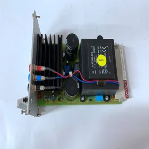
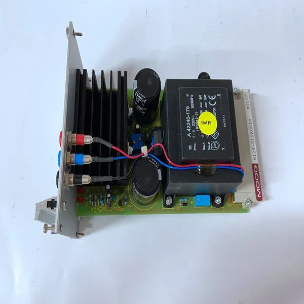
M128-010 M128-010-A001B
Related Products
Brand: MOOG
Type:M128-010 M128-010-A001B
Origin: the United States
Warranty: 365 days
Colour: new/used
Shipping method: Courier delivery
Module of PLC, DCS, ESD system card, the card is a vibration monitoring system, steam turbine control system module, the advantages of the gas generator spare parts brand: Allen Bradley, BentlyNevada, ABB, Emerson Ovation, Honeywell DCS, Rockwell ICS Triplex, FOXBORO, Schneider PLC, GE Fanuc, Motorola, HIMA, TRICONEX, Prosoft etc. Various kinds of imported industrial parts
Our main products are widely used in metallurgy, petroleum, glass, aluminum manufacturing, petrochemical industry, coal mine, papermaking, printing, textile printing and dyeing, mechanical, electronic manufacturing, automobile manufacturing, plastic machinery, electric power, water conservancy, water treatment/environmental protection, boiler heating, energy, power transmission and distribution and so on.
Memory Maps There are two points of view for memory maps: ❏ The mapping of all resources as viewed by local bus masters (local bus memory map) ❏ The mapping of onboard resources as viewed by VMEbus masters (VMEbus memory map) Local Bus Memory Map The local bus memory map is split into different address spaces by the Transfer Type (TT) signals. The local resources respond to the normal access and interrupt acknowledge codes. Normal Address Range The memory map of devices that respond to the normal address range is shown in the following tables. The normal address range is defined by the TT signals on the local bus. For the MVME162, transfer types 0, 1, and 2 define the normal address range. Table 3-1 defines the entire map ($00000000 to $FFFFFFFF). Many areas of the map are user-programmable, and suggested uses are shown in the table. The cache inhibit function is programmable in the MC68xx040 MMU. The onboard I/O space must be marked ‘‘cache inhibit’’ and serialized in its page table. Table 3-2 further defines the map for the local I/O devices.
 1. Reset enables the decoder for this space of the memory map so that it will decode address spaces $FF800000 - $FF9FFFFF and $00000000 - $003FFFFF. The decode at 0 must be disabled in the MCchip before DRAM is enabled. DRAM is enabled with the DRAM Control Register at address $FFF42048, bit 24. PROM/Flash is disabled at the low address space with PROM Control Register at address $FFF42040, bit 20. 2. This area is user-programmable. The DRAM and SRAM decoder is programmed in the MCchip, the local-to-VMEbus decoders are programmed in the VMEchip2, and the IP memory space is programmed in the IPIC. 3. Size is approximate. 4. Cache inhibit depends on devices in area mapped.

Send Inquiry to This Supplier


You May Also Like
-
PROMESS 850040060PUS$ 1031 - 2251MOQ: 1 Piece
-
WOODWARD 8701-758 5601-1126US$ 1031 - 2251MOQ: 1 Piece
-
IC698CMX016-ED VMIVME-5567-000 350-005567-000 EUS$ 1031 - 2251MOQ: 1 Piece
-
PFTL301E 3BSE019050R1000 1.0kNUS$ 1031 - 2251MOQ: 1 Piece
-
PROFIBUS DP-V1 ABCC-DPV1US$ 1032 - 2252MOQ: 1 Piece
-
VME172PA-652SEUS$ 1032 - 2252MOQ: 1 Piece
-
ZMI-2002 8020-0211-1-JUS$ 1032 - 2252MOQ: 1 Piece
-
E33NCHA-LNN-NS-00US$ 1032 - 2252MOQ: 1 Piece
-
LDP1WC/250P-16US$ 1032 - 2252MOQ: 1 Piece
-
TB852 3BSC950263R1US$ 1033 - 2253MOQ: 1 Piece


