








 Contact Platform Support
 Help Center
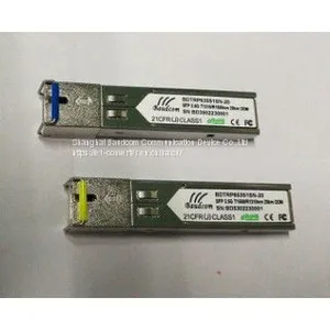
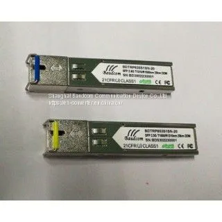
BDTRP695S1SD-40 2.5G SFP BIDI_1490nm_1550_40Km


Related Products
Baudcom’ BDTRP695S1SD-40, The SFP-BIDI transceivers are high performance, cost effective modules supporting dual data-rate of 2.5Gbps/2.125Gbps and 40km transmission distance with SMF.The transceiver consists of three sections: a DFB laser transmitter, a PIN photodiode integrated with a trans-impedance preamplifier (TIA) and MCU control unit. All modules satisfy class I laser safety requirements. The transceivers are compatible with SFP Multi-Source Agreement (MSA) and SFF-8472. For further information, please refer to SFP MSA.
Product Features
Supports 2.5Gbps/2.125Gbps bit rates
Bi-Directional LC connector
Hot pluggable SFP footprint
1490nm DFB laser and 1550nm PIN photo detector
1550nm DFB laser and 1490nm PIN photo detector
Applicable for 40Km SMF connection
Low power consumption
Digital Diagnostic Monitor Interface
Compliant with SFP MSA and SFF-8472
Very low EMI and excellent ESD protection
Operating case temperature:
Commerical:0 to 70 °C
Industrial:-40 to 85 °C
Functional Diagram Absolute Maximum Ratings Note: Stress in excess of the maximum absolute ratings can cause permanent damage to the transceiver. General Operating Characteristics Electrical Characteristics (TOP(C) = 0 to 70 ℃, TOP(I) =-40 to 85 ℃,VCC = 3.13 to 3.47 V) Notes: 1. TD+/- are internally AC coupled with 100Ω differential termination inside the module. 2. Tx Fault and Rx LOS are open collector outputs, which should be pulled up with 4.7k to 10kΩ resistors on the host board. Pull up voltage between 2.0V and Vcc+0.3V. 3.RD+/- outputs are internally AC coupled, and should be terminated with 100Ω (differential) at the user SERDES. Optical Characteristics (TOP(C) = 0 to 70 ℃, TOP(I) =-40 to 85 ℃,VCC = 3.13 to 3.47 V) Notes: 1.Measured at 2.5Gb/s with PRBS 2 223 – 1NRZ test pattern. 2.Unfiltered, measured with a PRBS223 – 1 test pattern @2.5Gb/s 3.Measured at 2.5Gb/s with PRBS 223 – 1 NRZ test pattern for BER -12 Pin Defintion And Functions Notes: 1.When high, this output indicates a laser fault of some kind. Low indicates normal operation. And should be pulled up with a 4.7 – 10KΩ resistor on the host board. 2. TX disable is an input that is used to shut down the transmitter optical output. It is pulled up within the module with a 4.7 – 10KΩ resistor. Its states are: Low (0 – 0.8V): Transmitter on (>0.8, High (2.0V~Vcc+0.3V): Transmitter Disabled Open: Transmitter Disabled 3.Mod-Def 0,1,2. These are the module definition pins. They should be pulled up with a 4.7K – 10KΩ resistor on the host board. The pull-up voltage shall be between 2.0V~Vcc+0.3V. Mod-Def 0 has been grounded by the module to indicate that the module is present Mod-Def 1 is the clock line of two wire serial interface for serial ID Mod-Def 2 is the data line of two wire serial interface for serial ID 4.When high, this output indicates loss of signal (LOS). Low indicates normal operation. 5.RD+/-: These are the differential receiver outputs. They are AC coupled 100Ω differential lines which should be terminated with 100Ω (differential) at the user SERDES. The AC coupling is done inside the module and is thus not required on the host board. 6. TD+/-: These are the differential transmitter inputs. They are AC-coupled, differential lines with 100Ω differential termination inside the module. The AC coupling is done inside the module and is thus not required on the host board. Digital Diagnostic Specifications The BDTRP695S1SD-40 transceivers can be used in host systems that require either internally or externally calibrated digital diagnostics. Notes: 1.When Operating temp.=0~70 ºC,the range will be min=-5,Max=+75 2. The accuracy of the Tx bias current is 10% of the actual current from the laser driver to the laser 3. Internal/ External Calibration compatible. Typical Interface Circuit Package Dimensions 

Send Inquiry to This Supplier

You May Also Like
-
155M~2.67Gbps ESFP Optical TransceiverUS$ 100 - 150MOQ: 1 Unit
-
1.25G SFP Optical Transceiver With DDM MornitorUS$ 100 - 150MOQ: 1 Unit
-
3Gbps Video SFP Optical Transceiver | SFP ModuleUS$ 100 - 150MOQ: 1 Unit
-
1.485Gbps Video SFP Optical TransceiverUS$ 100 - 150MOQ: 1 Unit
-
155M SFP Optical TransceiverUS$ 100 - 150MOQ: 1 Unit
-
155M SFP Optical TransceiverUS$ 100 - 150MOQ: 1 Unit
-
40Gb/s 40km QSFP+ TransceiverUS$ 100 - 150MOQ: 1 Unit
-
SFP+ Direct Attach Passive Copper CablesUS$ 80 - 150MOQ: 1 Unit
-
Hybrid Passive Copper 100GE QSFP28 to 4x 25GE SFP28US$ 80 - 150MOQ: 1 Unit
-
10G Bi-Directional SFP+ Optical TransceiverUS$ 100 - 150MOQ: 1 Unit


