

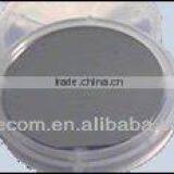
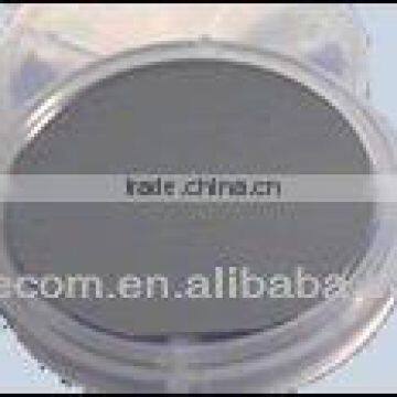
GaAs EPI Wafer
Negotiable
MOQ: 25 Pieces (Price negotiable depending on order volume and customization)
Key Specifications
Get Latest Price
Place of Origin:
Taiwan, China
Brand Name:
GaAs EPI Wafer
Payment & Shipping
Payment Methods:
Port of Shipment:
Taipei
Delivery Detail:
Delivery time depends on order quantity.
Related Products
-
 GaAs Wafer for LEDNegotiableMOQ: 25 Pieces
 -
AlGaInP RGB SMD Green LED ChipNegotiableMOQ: 1000 Pieces
-
Yellow LED Chip AlGaInP Wafer for SMDNegotiableMOQ: 1000 Pieces
-
Orange LED Chip AlGaInP Wafer for SMDNegotiableMOQ: 1000 Pieces
-
2" 4" 6" 2inch 4inch 6inch N-type Gallium Arsenide GaAs Wafer for Microwave/HEMT/PHEMTNegotiableMOQ: 25 Pieces
Place of Origin
Taiwan, China
Brand Name
GaAs EPI Wafer
Specifications
1. GaAs EPI wafer for LED/IR2. Growth Method MOCVD
3. GaAs wafer for Wireless Networking
4. GaAs EPI wafer for LD/PD
1. Description
This spec is apply to MOCVD process .
Product - AlGaInP MOCVD EPI Wafer
2. Spec
2.1 EPI Wafer Size
Growth |
MOCVD |
Diameter |
2” |
2.2 EPI Wafer Structure
High-Dopant p-GaP level |
100 – 300nm |
p-GaP Window level |
6 – 12um |
Emitting Area |
AlGaInP |
DBR |
DBR |
Substrate |
n-GaAs 350um |
2.3 EPI Wafer Parameter
Item |
Unit |
Red |
Yellow |
Yellow/Green |
Description |
|
|||||||||
Wave Length (λD) |
nm |
620 ~ 630 |
587 ~ 592 |
568 ~ 573 |
IF =20mA |
|
|||||||||
VF |
V |
< 2.2 |
< 2.2 |
< 2.2 |
Forward Voltage |
|
|||||||||
|
(Iv) |
mcd |
F |
70 – 80 |
F |
60-70 |
F |
10 – 15 |
IF =20mA |
||||||
|
G |
80 – 90 |
G |
70 – 80 |
G |
15 – 20 |
|||||||||
|
H |
90 – 100 |
H |
80 – 90 |
H |
20 – 25 |
|||||||||
|
I |
100 – 110 |
I |
90 – 100 |
I |
30 – 35 |
|||||||||
|
J |
110 – 120 |
J |
100 – 110 |
J |
35 – 40 |
|||||||||
|
K |
120 – 130 |
K |
> 110 |
K |
40 – 45 |
|||||||||
|
L |
130 – 140 |
|
|
L |
> 45 |
|||||||||
|
M |
> 140 |
|
|
|
|
|||||||||
Notes
- Wave Length and Luminous intensity can be changed by customer request.
- Luminous intensity data is based on the chip size test result that made from EPI Wafer,Red Led is base on 12×12mil2,Yellow and Yellow/Green Led are base on 8×8mil2 .The real electronic performance will be fully relied on chip process.

Send Inquiry to This Supplier

* Email
Want the best price?
Post an RFQ now!
Business Type
Manufacturer, Trading Company, Agent
Year Established
1998
Factory Size
10,000-30,000 square meters
Total Employees
11 - 50 People
You May Also Like
-
Intrinsic SemiconductorNegotiableMOQ: 2400 Pieces
-
New 12V 60W TEC1-12706 Thermoelectric Cooler Peltier Mini Thermoelectric Cooler and Warmer Thermoelectric Can CoolerUS$ 1 - 100MOQ: 100 Units
-
Temperature Indicator for Sputtering TargetUS$ 240 - 480MOQ: 10 Pieces
-
2012 NEW Scr Thyristor Module 200AUS$ 90 - 90MOQ: 1 Piece
-
RENESAS R5F1026AASP#55 Microcontroller Microcontroller ConverterUS$ 1 - 500MOQ: 1 Bag
-
Silicon Carbide (SiC) SubstratesUS$ 50 - 100MOQ: 10 Pieces
-
HEMT GaN On SiC For Power Wafer ManufacturersNegotiableMOQ: 15 Pieces
-
Control Unit Board H807ADPM H83DVCMM H807ADPE H831CCUC H835VDSHNegotiableMOQ: 1 Piece
-
Micro Porous Ceramic Suction Cup, Semiconductor Vacuum Suction Cup, Silicon Carbide Alumina Dense Ceramic Turntable Suction CupNegotiableMOQ: 100 Pieces
-
Manual Multi-function Die Bonder Eutectic and Epoxy Bonding in One SystemUS$ 20000 - 30000MOQ: 1 Piece


