








 Contact Platform Support
 Help Center
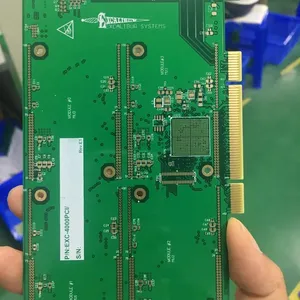
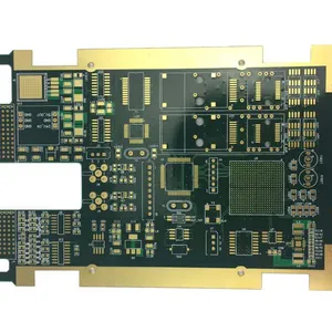
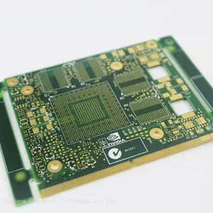
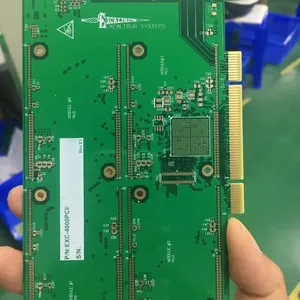
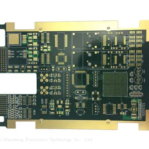
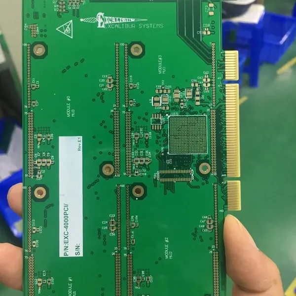
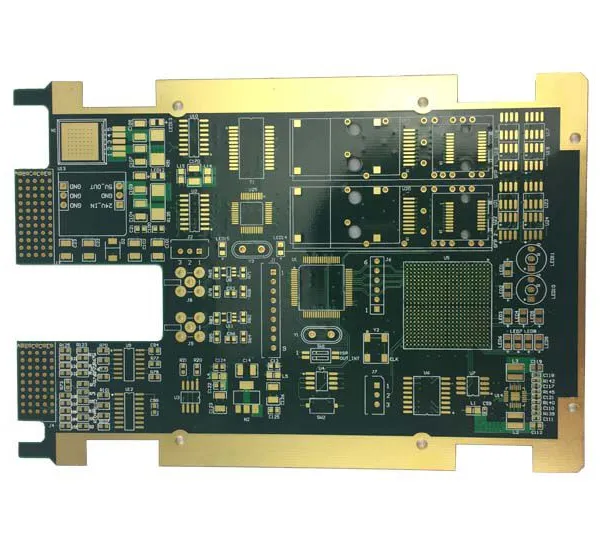
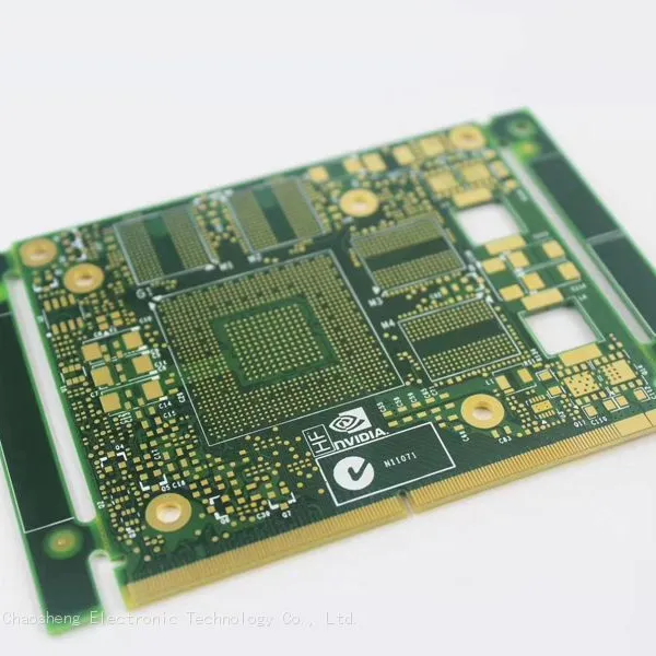
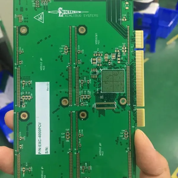
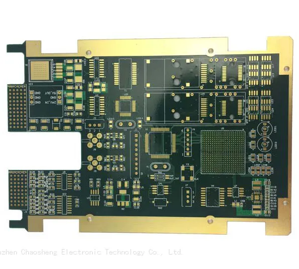
Double‑sided PCB With Gold Finger
Product Spotlights



Related Products
-
 China Chaosheng Electronic Server Graphics Multi Layer Gold Finger Circuit Board PCBNegotiableMOQ: 1 Blade
 -
China Chaosheng Electronic Computer Memory Module Multi Layer Gold Finger Circuit Board PCBNegotiableMOQ: 1 Blade
-
China Chaosheng Electronics Desktop Computer Memory Module Multi-layer Gold Finger Circuit Board PCBNegotiableMOQ: 1 Blade
-
China Chaosheng Electronics Desktop and Pen Computer Memory Module Multi Layer Gold Finger Circuit Board PCBNegotiableMOQ: 1 Blade
-
2-layer SG Card, SD Card, Thick GoldPCB,Multi Layer Ultra-thin PCBNegotiableMOQ: 20 Units
If you have any needs, please feel free to contact China Chaosheng Electronics Company. Please contact us as follows:
whatsapp:+8613528819118
Skype live: pcb-fpcb88@163.com
E-mail : sales@chaoshengpcb-fpc.com
Contact: Mank. Li
China Chaosheng Electronic Computer Graphics Card Multi layer Gold Finger Circuit Board PCB
China Chaosheng Electronics specializes in PCIe4.0/5.0 graphics card high-speed multi-layer PCB and dedicated electric hard gold finger technology, which is compatible with gaming graphics cards, AI computing power graphics cards, and professional graphics cards. It integrates a complete set of processes including high-speed HDI blind hole embedding, impedance control, selective electroplating hard gold, and stepped contact forming. Below is a complete breakdown of the board architecture, gold finger coating process, full process manufacturing, performance parameters, special quality control, and GPU PCB customization solution.
1、 Multi layer architecture technology for graphics card PCB substrate
1. Stacking and Layer Specification
1. Conventional gaming graphics card: 8-12 layer HDI board of any order; High end AI computing graphics cards achieve 14-24 layer high-order blind buried hole structure, supporting 0.3mm ultra-fine pitch BGA memory and GPU chip packaging
2. Board substrate: Select high TG-170 FR-4, halogen-free board, and high-frequency low loss board; High power graphics card with thickened inner copper foil (2oz -4oz thick copper), carrying high current power supply for GPU, reducing power impedance and suppressing heat generation
3. The laminated alignment tolerance is ≤± 10 μ m, and multiple presses are used to prevent delamination of the board in high-temperature working environments; Control depth drilling and micro blind hole with a minimum aperture of 0.075mm and a hole wall roughness of ≤ 20 μ m to ensure high-speed signal communication
2. Design process for high-speed signal integrity
1. PCIe X16 gold finger impedance precise control: differential signal impedance of 100 Ω, single ended signal of 50 Ω, tolerance of ± 5 Ω
2. Long short ladder style gold finger contact arrangement: the grounding contact is the longest, the power contact is centered, and the high-speed signal contact is the shortest; When powered on, the ground wire is connected first to prevent surge from penetrating the GPU core chip, and is compatible with hot swappable protection standards
3. Power segmentation and complete planning of reference layer to reduce crosstalk and meet the PCIe5.0 single channel 16Gbps transmission bandwidth
2、 Core technology of graphics card gold finger (electric hard gold) coating
The graphics card plug-in interface * * prohibits ordinary immersion gold and soft gold * *. Chaosheng Electronics adopts a three-layer composite structure of selective electrolytic electroplating hard gold (gold cobalt alloy coating), which is the key to the wear resistance and oxidation resistance of the graphics card interface
The coating has a three-layer structure from inside to outside
1. Copper based bottom layer * *: PCIe contact copper strip formed by etching the board edge, with a copper foil thickness of 35-70 μ m
2. Nickel barrier transition layer (electroplated nickel) * *: thickness 3-5 μ m; Isolate the mutual diffusion of copper and gold atoms, prevent copper precipitation at high temperatures from causing blackening and poor contact of gold fingers, and improve the hardness of the coating
3. Surface electroplating of hard gold Au Co alloy**
-Consumer grade gaming graphics card: Gold thickness 1.27 μ m (50uinch)
-AI server graphics card, industrial graphics card: thickened hard gold 1.8-2.54 μ m (75-100uinch)
-The hardness of the coating is HV180-220, the wear resistance is more than 8 times that of ordinary immersion gold, and the insertion and removal life is ≥ 1000 times; Gold purity ≥ 99.9%, stable contact resistance
Selective electroplating exclusive process
1. The outer circuit etching is completed, the solder mask ink window is opened, and the gold finger area must not be covered with green oil**
2. Use specialized electroplating fixtures and blue adhesive masks to cover the remaining solder pads of the PCB, and only electroplate the edge contact points of the board to prevent excessive gold plating in excess positions
3. Precise cutting of electroplated leads after installation, with a flat incision that does not damage the contacts; The gold finger insertion end is uniformly chamfered at a 45 ° angle, ensuring smooth insertion and removal without scratching the motherboard slot spring
3、 Complete production process flow
Multi layer inner layer lamination → CNC micro hole drilling → PTH copper plating → outer layer circuit exposure etching → impedance testing → solder mask printing, gold finger window opening → text screen printing → selective nickel plating+hard gold plating → board edge forming, gold finger 45 ° chamfering → electroplating lead cutting → gold finger protective film coating → flying pin on/off testing, X-RAY blind buried hole testing → impedance sampling, coating thickness testing → appearance AOI quality inspection → anti-static packaging and shipping
4、 Special Quality Control Standards for Graphics Card PCB
1. The thickness tolerance of the gold finger coating is ≤± 10%, the surface roughness of the contact is Ra ≤ 0.05 μ m, and there are no pinholes, scratches, exposed nickel, or oxidation spots
2. The copper wall of the blind buried hole is intact, the copper filling rate inside the hole is ≥ 95%, and there are no voids
3. High and low temperature cycling, wet heat aging test: cycled 500 times from -40 ℃ to+125 ℃, the gold finger coating does not peel off or peel off
4. Salt spray corrosion resistance test, insertion and removal wear resistance life test, full inspection
5、 Chaosheng can customize graphics card PCB categories
1. Consumer gaming graphics card: 8-12 layer HDI, PCIe 4.0 X16 gold finger circuit board
2. AI computing power acceleration card: 14-24 layer high multi-layer, thick copper power supply, thick wear-resistant hard gold finger PCB
3. Industrial and vehicle mounted independent display: high temperature resistant halogen-free substrate, military grade thickened electroplated gold fingers
4. Customization of software and hardware integrated graphics card boards, aluminum based heat dissipation graphics card substrates
6、 Compared to ordinary gold-plated PCBs, electroplated hard gold fingers have advantages
|Process type | Coating material | Wear resistant plug life | Applicable scenarios|
|Electroplated hard gold (standard for Super Sheng graphics cards) | Gold cobalt alloy | ≥ 1000 insertions/removals | PCIe graphics cards, pluggable cards|
|Chemical immersion soft gold | Pure gold thin layer | < 80 times | BGA solder pad, cannot be used as a plug-in contact|

Send Inquiry to This Supplier



You May Also Like
-
Mobile Phone Motor 2-layer Ultra-thin Carbon Oil PCB,Apple Phone Ultra-thin Charging Head PCBNegotiableMOQ: 20 Units
-
2-layer Ultra-thin Ultra Large Size PCB,Ultra Thin and Ultra Large Size PCBNegotiableMOQ: 5 Units
-
2-layer Thin Plate+thick Metal+high Carbon ResistancePCB,Micro Motor Ultra-thin High Carbon Resistance PCBNegotiableMOQ: 200 Units
-
6-layer HDI Ultra-thin Convex High and Low Copper Circuit Board PCB,Microphone Ultra-thin Step PCBNegotiableMOQ: 100 Blades
-
4-layer Ultra-thin Charging Head PCB for Mobile Phones of Any OrderNegotiableMOQ: 200 Units
-
2-layer Ultra-thin Convex High and Low Copper Circuit Board PCB,0.20mm High and Low Copper Bump PCBNegotiableMOQ: 10000 Units
-
SG Card Ultra-thin 2-layer HDI Thick Gold Finger PCB,Multi Layer Ultra-thin HDIPCBNegotiableMOQ: 200 Blades
-
2-layer Light Strip Thin Circuit Board PCB,Ultra Thin Gold Finger Thick Gold PCBNegotiableMOQ: 10 Blades
-
4-layer Universal Circuit Board PCB,Ajinomoto Build-up FilmPCBNegotiableMOQ: 1 Blade
-
4 Layers of Ultra-thin Thick Gold Circuit Board PCB for Mobile Phone CardsNegotiableMOQ: 1000 Blades


