

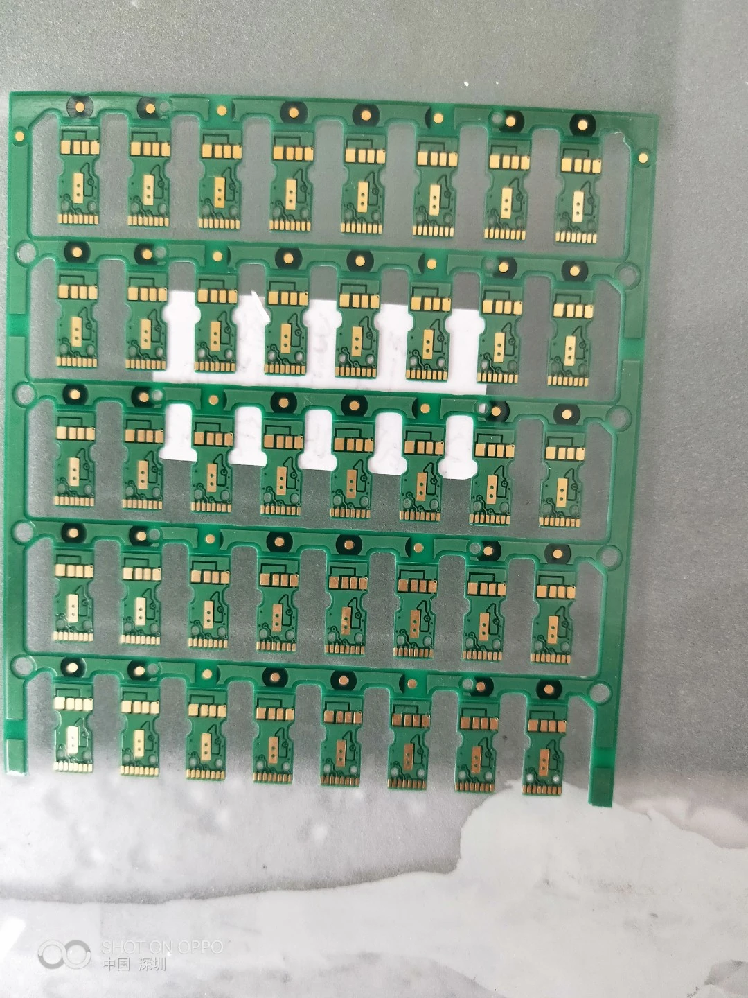
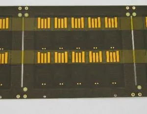
2-layer SG Card, SD Card, Thick GoldPCB,Multi Layer Ultra-thin PCB

Related Products
-
 Mobile Phone Motor 2-layer Ultra-thin Carbon Oil PCB,Apple Phone Ultra-thin Charging Head PCBNegotiableMOQ: 20 Units
 -
2-layer Ultra-thin Ultra Large Size PCB,Ultra Thin and Ultra Large Size PCBNegotiableMOQ: 5 Units
-
2-layer Thin Plate+thick Metal+high Carbon ResistancePCB,Micro Motor Ultra-thin High Carbon Resistance PCBNegotiableMOQ: 200 Units
-
6-layer HDI Ultra-thin Convex High and Low Copper Circuit Board PCB,Microphone Ultra-thin Step PCBNegotiableMOQ: 100 Blades
-
4-layer Ultra-thin Charging Head PCB for Mobile Phones of Any OrderNegotiableMOQ: 200 Units
Product application: Apple phone charging head
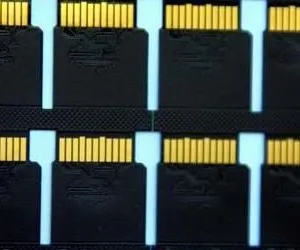
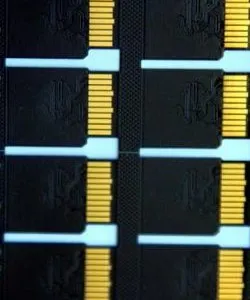
Layers: 2-layer SG card, SD card, thick gold sheet PCB
Board: FR-4, TG150, inner and outer copper thickness of 1OZ
Minimum aperture: 0.20mm
Through-hole/
Minimum line width: 4mm
Minimum line width: 4mil
Minimum pore copper: 15um
Minimum laser hole/mm
Impedance:+-10%
Finished copper: 1OZ
Finished product thickness 0.20mm
Shipping size: 136.0 * 115mm/6 * 8PCS
Surface treatment: 1u immersion gold+20u electroplated nickel gold
Transport Package:Vacuum packaging+separated white paper+moisture-proof beads
Main Product Structure of Chaosheng Group Company
2-80 layers of rigid circuit boards, 2-50 layers of flexible circuit boards and PCBA production
Chaosheng Group Company mainly produces product categories
High end double-sided, multi-layer, flexible, high-frequency, HDI interconnect, metal based, high thermal conductivity metal based, ceramic, cut in metal based, cut in buried capacitor, cut in thick copper buried magnet, concave convex step substrate, 5G high-speed board, thick copper, thick gold, high carbon resistance, double-sided multi-layer MiNiLED, MiNiHDILED, MiNiOLED, IC carrier substrate, roll to roll FPC, long FPC, large-sized printed circuit board, halogen-free material, high-frequency material, high-speed material, metal material, environmentally friendly circuit board, blind buried hole circuit board, high thermal conductivity aluminum based, thermoelectric separation copper based, PDU busbar, iron-based and metal based (core) mixed pressure plate, embedded copper buried copper. Buried resistance buried capacitance buried ceramic bead board, ultra-thin BT board, ceramic substrate, IC carrier board, high-frequency mixed voltage, high-speed board, differential impedance board, thick copper plate, thick gold plated board, HDI An integrated OEM and ODM production factory for Anylayer, double-sided, multi-layer, HDI FPC, soft hard combination HDI, roll to roll FPC, ultra long FPC, ultra large size PCB production and product design and development, software development, special material printed circuit boards, etc.
The main application areas of PCB and PCBA products of Chaosheng Group Company
Communication terminals, communication stations, electronic communication, fiber optics, optical modules, backlight sources, chip systems, communication equipment, communication instruments, computers, intelligent devices, intelligent control, system control, industrial power control, industrial equipment, testing instruments, testing instruments, SD cards, SG cards, mobile phones, computers, various antennas, radars, automobiles, light sources, resistors, music equipment, playback equipment, banking equipment, medical instruments, medical equipment, aerospace, aviation, military, LED, OLED, OLCD power control power supply, industrial power supply, communication power supply, automotive power supply, office equipment, digital products, computers and other application fields;
The main application areas of flexible circuit boards (FPC) and FPCA products of Chaosheng Group Company
Hard drives, printers, fax machines, scanners, sensors, mobile phones, connectors, modules, walkie talkie antenna cards, high-end cameras, digital cameras, laser heads, CDs, medical devices, instruments, drives, automobiles, automotive instruments, automotive drive disks, drivers, optical drives, medical devices, medical equipment, backlight sources, modules, banking equipment, industrial instruments, LED light strips, military, aviation, aerospace, national defense and other product fields.
If you have any needs, please contact us:
whatsapp:+8613528819118
Skype live: pcb-fpcb88@163.com
E-mail : sales@chaoshengpcb-fpc.com
Contact: Mank. Li
The specifications for DDR4 generation 16G desktop computer memory modules are as follows:
• Memory type: DDR4, which is currently the mainstream memory type, has a higher data transfer rate and lower power consumption compared to DDR3.
• Capacity: 16GB, common forms of composition include single 16GB or a set of two 8GB.
• Main frequency: Common main frequencies include 2133MHz, 2400MHz, 2666MHz, 3200MHz, etc.
Voltage: The standard operating voltage is generally 1.2V. Low voltage design can reduce power consumption and heat generation, improve system stability and service life.
Pin count: usually 288 pins, using DIMM slot type, strong compatibility, suitable for various desktop motherboards.
CL latency: The CL latency of memory with different clock frequencies varies, for example, for 2666MHz memory, the CL latency may be 19-19-433200MHz memory, and the CL latency may be 22-22-22.
Module type: Generally UDIMM (Unbuffered Memory Module), can only be installed in desktops/workstations that support DDR4 DRAM.
• Heat dissipation design: Some high-end or high-frequency DDR4 16G memory modules are equipped with heat sinks to help dissipate heat and ensure the stability of the memory during high load operation. For example, Crucial DDR4 Pro uses an integrated narrow version heat sink.
Memory module models are mainly divided into three dimensions: technical generation (DDR series), physical specifications (DIMM/SO-DIMM, etc.), and functional types (ECC/RDIMM, etc.). The following is a detailed explanation of the mainstream models:
1. According to technical generation (core model, determining compatibility), this is the most critical classification. Different generations have incompatible physical interfaces and must be matched with the motherboard. Table Generation Release Time Mainstream Frequency Operating Voltage Characteristics Application Scenarios DDR5 2020 4800-8400 MT/s
1.1V Bandwidth Doubling, Lower Power Consumption, Larger Single Line Capacity (up to 128GB+), Supports On die ECC New Platform Desktop, Laptop, Server DDR4 2014 2133-4000 MT/s
1.2V Mainstream, Good Compatibility, High Cost Performance Mainstream Desktop, Laptop, Server DDR3 2007 1066-2133 MT/s 1.5V Old Platform Standard, Gradually Eliminated Old Computers and Some Industrial Control Equipment DDR2 2003 400-800 MT/s 1.8V High Power Consumption, Small Capacity, Basically Eliminated Goodwin Class Computers DDR1 2000 200-400 MT/s 2.5V Early Double Rate Memory, Already Eliminated Early Pentium mobile low-power versions: LPDDR5/LPDDR4/LPDDR3, Specially designed for mobile phones, tablets, and ultrabooks, with lower voltage and lower power consumption.
2、 The physical specifications (size and interface) determine whether the memory can be installed into the device, and the size and pin count are different. UDIMM (Unbuffered DIMM): Standard desktop memory, large size, 288 pins (DDR4/DDR5), no buffering chip, low latency, low cost, mainstream for home/office use. SO-DIMM (Small DIMM): specifically designed for laptops/mini consoles, with a size of approximately half of UDIMM, 260 pins (DDR4)/262 pins (DDR5), saving space. RDIMM (Registered DIMM): Server memory with register chip, reduces CPU load, supports stable operation of multiple memory slots, and supports ECC error correction. LRDIMM (Reduced Load DIMM): High end server memory that goes further than RDIMM, buffers data signals, supports ultra large capacity (single 256GB+), and is used for virtualization and memory databases. CAMM2: a new generation of laptop memory form, replacing SO-DIMM, thinner, better heat dissipation, and stronger scalability, gradually becoming popular.
3、 ECC memory by function and special type: with error checking function, automatically fixes data errors, improves stability, used for servers and workstations, not supported by ordinary home motherboards. Non ECC memory: No error correction function, mainstream for home/consumer use, lower cost. RGB gaming memory: Essentially UDIMM, with RGB lighting effects and overclocking optimization, suitable for DIY gaming consoles, balancing appearance and performance. NVDIMM: Non volatile memory, data is not lost during power outages, used for enterprise level critical data storage, and is expensive.
4、 Common Model Naming Rules (Taking DDR4 as an Example) DDR4-3200 16GB UDIMM • DDR4: Technical Generation • 3200: Data Transfer Rate (MT/s) • 16GB: Capacity • UDIMM: Physical Specifications
|
Process Capability Table | ||||
| Technical ltem | MassProduct | Advanced Technology | ||
| 2015 | 2021 | 2025 | ||
| Max.Layer Count | 80 layer | 100 layer | 100 layer | |
|
PCB through hole board |
2~80 layer | 2~100 layer | 2~100 layer | |
|
Maximum size through hole 1~2 |
37〞*98.50" | 43.3〞*118.11" | 43.3〞*118.11" | |
|
Minimum line width and spacing |
10(0.40) | 10(0.40) | 7.50(0.30mm) | |
| Minimum mechanical hole(mm) |
12(0.50) | 10(0.40) | 8.50(0.35mm) | |
|
Maximum size through hole 4~22 layers |
37〞*43.30" | 43.3〞*43.30" | 43.3〞*43.30" | |
|
Maximum size through hole 4~22 layers |
31.50 ″*59" | 31.50 ″*70.86" | 31.50 ″*70.86" | |
|
Maximum size through hole 4~22 layers |
10(0.40) | 10(0.40) | 7.50(0.30mm) | |
| Minimum line width and spacing for multi-layer large-sized PCBs |
10(0.40) | 10(0.40) | 7.50(0.30mm) | |
|
Maximum size of multi-layer through- hole : 4-22 layers with the smallest hole |
12(0.50) | 10(0.40) | 8.50(0.35mm) | |
| Maximum size HDI 4~36 layers | 31.50 ″*55" | 31.50 ″*55" | 31.50 ″*55" | |
| Minimum line width and line spacing of large size PCB |
Through hole 12 / 12milHDI14 /14mil |
Through hole 10/10 milHDI12 / 12mil |
Through hole 8 / 8milHDI12 / 12mil |
|
| The largest board ruler 1 → the smallest hole of 18 layers |
Through hole 0.50mmHDI :0.45mm |
Through hole 0.50mm HDI : 0.45mm |
Through hole 0.50mmHDI : 0.45mm |
|
| The layer number of FPC | 1~36layer | 1~60layer | 1~60layer | |
| Maximum size of flexible FPC |
19.68〞*55" | 28〞*59" | 31.49〞*118.12" | |
| Maximum size of flexible FPC with soft hard combination |
19.68〞*55" | 28〞*59" | 31.49〞*118.12" | |
|
FPC (roll to roll) maximum size |
19.68 ″*7874" | 19.68 ″*7874" | 19.68 ″*7874" | |
|
Maximum size of FPC single chip shipment |
19.68 ″*118.11" | 19.68 ″*196.8" | 19.68 ″*196.80" | |
| The layer number of FPC | 2~18 layer | 2~36 layer | 2~42 layer | |
|
Maximum size of layered board |
19.68 ″*35" | 19.68 ″*43" | 19.68 ″*43" | |
|
Number of through-hole layers |
2~20layer | 2~30 layer | 2~40 layer | |
|
Hard and soft HDI layers |
2~14 layer | 2~18 layer | 2~22 layer | |
|
Maximum size of soft and hard combination |
19.68 ″*43" | 19.68 ″*49" | 19.68 ″*49" | |
|
FPC/soft-hard combination arbitrary interconnection HDI |
4+X+4Interconnect HDI |
5+X+5Interconnect HDI | 6+X+6Interconnect HDI |
|
|
HDIPCB layers |
4~36layer | 4~60layer | 4~80 layer | |
|
Anylayer HDI PCB |
4+X+4Interconnect HDI |
5+X+5、Interconnect HDI | 8+X+8、Interconnect HDI |
|
|
HDIPCB maximum board size |
24"*52" | 43"*49" | 43"*49" | |
|
Number of through hole layers of high frequency board |
2~18 layer | 2~36 layer | 2~60 layer | |
| HDI layers ofhighfrequency board |
2~16 layer | 2~24 layer | 2~60layer | |
| Maximum size of high frequency board |
37 ″*43" | 43 ″*49" | 43 ″*49" | |
|
Number of ceramic plates |
1-2 layer | 1~4 layer | 1~6 layer | |
|
Ceramic plate thickness |
0.60mm-1.60mm | 0.38mm-20.0mm | 0.38mm-20.0mm | |
|
Maximum size of ceramic plate |
100*150mm | 150*190mm | 150*650mm | |
|
Minimum aperture of ceramic plate |
0.50mm | 0.35mm | 0.35mm | |
|
Minimum line width and line spacing of ceramic board |
16/16mil | 12/12mil | 10/10mil | |
|
Number of layers of metal copper substrate |
1-2 layer | 1~4 layer | 1~6 layer | |
|
Maximum line width and line spacing of metal iron substrate |
12/12mil | 4/4mil | 4/4mil | |
|
Number of layers of metal aluminum substrateHDI |
1-2 layer | 1~4 layer | 1~6 layer | |
|
Maximum size of metal substrate |
37 ″*43" | 25.59 ″*59" | 25.59 ″*59" | |
| The smallest hole of the metal substrate |
0.50mm | 0.35mm | 0.35mm | |
|
Minimum line width and line spacing of metal substrate |
8/8mil | 4/4mil | 4/4mil | |
| Transparent FR- 4 material layers |
1-2layer | 1-2layer | 1-8layer | |
| Transparent FR-4 minimum hole |
0.35mm | 0.35mm | 0.35mm | |
| Transparent FR-4 minimum line width and spacing |
4/4Mil | 4/4Mil | 3.5/3.5Mil | |
| Transparent FR- 4 maximum size |
23.63*47.25″ | 23.63*47.25 ″ | 23.63*47.25 ″ | |
| Number of tempered glass base layers |
1-2layer | 1-2layer | 1-2layer | |
| Minimum line width and spacing of glass |
4/4Mil | 4/4Mil | 3.5/3.5Mil | |
| The smallest hole in glass |
0.35mm | 0.35mm | 0.35mm | |
| Maximum size of glass |
23.63*47.25″ | 23.63*47.25 ″ | 23.63*47.25 ″ | |
| Number of layers of transparent PETmaterial |
1-2layer | 1-2layer | 1-2layer | |
| Maximum size of transparent PET |
19.68 ″*7874" | 19.68 ″*7874" | 19.68 ″*7874" | |
|
The company's main product types |
Halogen free materials, high TG materials, high-frequency materials, high-speed materials, metal materials, glass materials, embedded materials, transparent FR- 4 materials, high thermal conductivity metals, high thermal conductivity aluminum substrates, environmentally friendly circuit boards, BT materials, ABF materials, and other imported materials, DU busbars, iron-based and metal based (core) mixed pressure plates, embedded buried copper, buried resistors, buried capacitors, buried ceramic bead plates, buried ceramics, ceramic mixed pressure plates, multi-layer ceramics, ultra-thin BT plates, ultra-thin PCBs, ultra-thin PCBs, multi-layer aluminum substrates, multi-layer ceramic plates, multi-layer ultra-thin HDI、 High frequency mixed voltage, differential impedance board, thick copper plate, gold-plated plate, high and low copper, high and low copper, high carbon resistance, transparent multilayer, glass plate, HDI arbitrary order (cross blind buried) Anylayer, flexible double-sided, flexible multilayer, soft hard combination HDI, roll to roll FPC, ultra long size, ultra large size board (single, double, multi-layer) PCB production and product design, product development, software development, etc |
|||
| Main material |
Rogers, Taikoni, Yaron, Mitsui, Isola, 3M, Taiyao, Taiguang, Tenghui, Shengyi,Lianmao, Nanya, Doosan, DuPont, Taihong, Hongren, Xinyang, Nippon Steel, Teflon,Yasen, Panasonic, RCC, Mitsui, Mitsubishi, Yingye, 3M, Kyocera, Jiuhao, Zhongci,Huaqing, Aishengda, Sliton, Kaichangde, Tongxin, Beige, Yalong, Taikoni,Hitachi, Laird System, etc |
|||
|
Main material categories |
Halogen-free、halogenated、 high thermal conductivity, high TG135 、TG140、 TG150、 TG170、TG180、TG240、TG320 |
|||
| Build-up Material | FR-4 ,TG150,TG70,TG180 | |||
| Conventional plate thickness (mm) |
Min.1-2L(mm) | 0.10mm | 0.10-12.0mm | 0.10-18.0mm |
| Min.4-10L(mm) | 0.35mm | 0.35mm~10.0mm | 0.35-18.0mm | |
| Min.12L(mm) | 0.43 | 0.38~10.0mm | 0.38~18.0mm | |
| Min.16L(mm) | 0.53 | 0.45~10.0mm | 0.45~18.0mm | |
| Min.18L(mm) | 0.63 | 0.51~10.0mm | 0.51~18.0mm | |
| Min.52L(mm) | 0.8 | 0.65~10.0mm | 0.65~18.0mm | |
| MAX(mm) | 3.5 | 12.0mm | 18.0mm | |
|
Copper plate thickness and copper thickness |
1-2 layerCU | 700um | 875um | 875um |
| Layers 4-20 |
4-12layer | 4-16layer | 4-22layer | |
| Inner layer copper thickness(um) |
875um | 1050um | 1225um | |
|
Outercopperthickness |
210um | 350um | 525um | |
|
Thick copper finished plate thickness |
8.0mm | 12.0mm | 18.0mm | |
| IC substrate |
layerHDI | 1-10layer | 1-14layer | 1-16layer |
| Line width and spacing |
50um | 25um | 15um | |
| copper thickness |
8-10um | 10-12um | 12-15um | |
| Min.CoreThickness um(mil) | 254" (10.0) | 0.15~254(10.0mm) | 0.15~254(10.0mm) | |
| Min.Build up Dielectric |
38(1.5) | 25(1.0) | 25(1.0) | |
|
BaseCopperWeigh t |
Inner Layer | 1/4-8 OZ | 1/4-0.30mm | 1/4-0.30mm |
| Out Layer | 1/4-10 OZ | 1/4-30 OZ | 1/4-30 OZ | |
| Gold thick | 1~40u" | 1~200u" | 1~200u" | |
| Nithick | 76~127u" | 1~250u" | 1~250u" | |
|
Min.HOle/Land um(mil) |
150/300(6/12) | 100/200(4/8) | 100/200(4/8) | |
|
Min.Laser via/landum(mil) |
60/170(2.4/6.8) | 50/150(2/6) | 50/150(2/6) | |
|
Min. IVH、Hole size/landum(mil) |
150/300(6/12) | 100/200(4/8) | 100/200(4/8) | |
| DieletricThickness | 38(1.5) | 32(1.3) | 32(1.3) | |
| 125(5) | 125(5) | 125(5) | ||
| SKipvia | Yes | Yes | Yes | |
| viaoNhie(laserviaon BuriedPTH) | Yes | Yes | Yes | |
| Laser Hole Filling | Yes | Yes | Yes | |
| Technicalltem | MassProduct | Advanced Technology | ||
| Hole depth/diameter | Through Hoie | 25:01 :00 | 35:01 :00 | 40:01 :00 |
| AspctRatio | MicroVia | 0.8 :1 | 0.8 :1 | 0.8 :1 |
| copperFilling Dimple Size | 10(0.40) | 5(0.20) | 5(0.20) | |
|
Minimumouter line width/ spacing |
Inner layer line width and spacing | 38/38(1.5/1.5) | 38/38(1.5/1.5) | 38/38(1.5/1.5) |
|
PlatedLayerum(mil) |
38/38(1.5/1.5) | 38/38(1.5/1.5) | 38/38(1.5/1.5) | |
| BGAPitchmm(mil) | 0.4 | 0.4 | 0.4 | |
| PHMin.Hole rlng um(mil) | 75(3) | 62.50(2.50 | 62.50(2.50 | |
| Line Width control |
±0.50 | ±0.50 | ±0.50 | |
| 2.5mil≤L/W | ±0.50 | ±0.50 | ±0.50 | |
| ≤3mil(mil) | ±0.60 | ±0.60 | ±0.60 | |
| SolderMask Registration um(mil) |
±25 | ±25 | ±25 | |
| Solder masThickness |
Lines Minum(mil) | 10(0.40) | 10(0.40) | 10(0.40) |
| Lines Minum(mil) | 30(1.20) | 30(1.20) | 30(1.20) | |
| CopperMinum(mil) | 10(0.40) | 10(0.40) | 10(0.40) | |
| CopperMax um(mil) |
30(1.20) | 30(1.20) | 30(1.20) | |
| Mln.Solder Mask opening um(mil) |
250(10) | 200(8) | 200(8) | |
|
Structure |
Stacking layer by layer |
5+N+5 | 6+N+6 | 7+N+7 |
| Sequenetlal Bu il-up | 42Any Layer | 46Any Layer | 60Any Layer | |
| Stacking layer by layer |
N+N | N+N | N+N | |
| N+X+N | N+X+N | N+X+N | ||
| Sequenetlal Lamination |
4+(N+X+N)+4 | 5+(N+X+N)+5 | 6+(N+X+N)+6 | |
|
Multi-layer stepped structure |
Multi- layer stacking |
5+N+5 | 6+N+6 | 7+N+7 |
| Sequenetlal Bu il-up | 12Any Layer | 16Any Layer | 18Any Layer | |
| Multi- layer staircase |
4 steps | 6 steps | 6 steps | |
| Mechanical depth control drilling depth |
2.0mm±0.08mm | 2.0mm±0.08m | 2.0mm±0.08m | |
| Laser controlled depth drilling |
0.6mm±0.08mm | 0.8mm±0.08mm | 1.0mm±0.08mm | |
|
/Min.HOle/Land um(mil) |
linner um(mil) | 150/300(6/12) | 100/200(4/8) | 100/200(4/8) |
| Outer um(mil) | 150/300(6/12) | 100/200(4/8) | 100/200(4/8) | |
|
Minimumburiedholediameter/solder pad |
60/170(2.4/6.8) | 50/150(2/6) | 50/150(2/6) | |
| SUBDielectricThic kness |
Mln.um(mil) | 38(1.5) | 32(1.3) | 25(1.0) |
| Max.um(mil) | 125(5) | 125(5) | 125(5) | |
| SKipvia | Yes | Yes | Yes | |
| Via on hole(LaserViaon BuriePTH | Yes | Yes | Yes | |
| Laser Hole Filling | Yes | Yes | Yes | |
|
Resin plug hole plate thickness |
Min mm(mil) | 0.35 | 0.35 | 0.35 |
| Max mm(mil) | 3.2 | 3.2 | 3.2 | |
| Min mm(mil) | 125(5) | 110(4.50) | 110(4.50) | |
| Routing Depth control Accuracy um(mil) |
±50um(mil) | ±50um(mil) | ±50um(mil) | |
| Outine NC Rcuting Tolerance um(mil) |
75(3) | 75(3) | 75(3) | |
|
Type of surface Finishing |
OSP、 Sinking gold, lead-free tin, lead tin, electroplated gold fingers, electroplated gold (electroplated nickel hard gold, electroplated nickel soft gold), gold fingers+sinking gold, spray tin+gold fingers, OSP+electroplated gold, OSP+sinking gold, electroplated silver, electroplated silver, electroplated tin, gold coated silver, nickel free electroplated thick gold, nickel free electroplated thick silver, tin silver copper, OSP+gold fingers |
|||
| EN Thickness Control(um) |
>0.025-0.1um | >0.025-0.1um | >0.025-0.1um | |
| OSOSP Thickness(um) | >0.20-0.50um | >0.20-0.50um | >0.20-0.50um | |
| Ni Thickness(um) |
>105⇢ 250um | >105⇢ 250um | >105⇢ 250um | |
| Platinum thickness control |
>0.025-5um | >0.025-5um | >0.025-5um | |
| Lead/lead- free tin spraying thickness |
>105⇢ 150um | >105⇢ 150um | >105⇢ 150um | |
| Electrosilver | >105⇢ 140um | >105⇢ 140um | >105⇢ 140um | |
| Thickness control of sinking silver |
>105⇢ 140um | >105⇢ 140um | >105⇢ 140um | |
| Tin thickness control |
>105⇢ 140um | >105⇢ 140um | >105⇢ 140um | |
|
Min TestPAD |
E/Tum(mil) | 75(3) | 75(3) | 75(3) |
| E/Tum(mil) | 50(2) | 50(2) | 50(2) | |
| E/Tum(mil | 25(1) | 25(1) | 25(1) | |
| E/Tum(mil) | 150(6) | 150(6) | 150(6) | |
|
lmpedanceContro lTolerance |
≧50ohm | ± 10% | ±8% | ±8% |
| ≦50ohm | ±50ohm | ±50ohm | ±50ohm | |
| Finished board | Plate thickness≧0.15mm | ≧ ± 10% | ≧ ± 10% | ≧ ± 10% |
| Plate thickness≧0.15mm | ≧ ±0.075% | ≧ ±0.075% | ≧ ±0.075% | |
| Warpage | ≤0.7% | ≤0.5% | ≤0.5% | |
| The above are the conventional production skills of Chaosheng Group Company, and there are any unclear points. Please further communicate with our specialized technical personnel, and we will be happy to serve you! Welcome to our guide! | ||||
FAQ
Question Point Answer
Q: What information is required for PCB CEGSATE: Gberber files for PCB production, product process instructions, such as material requirements, surface treatment requirements, finished product thickness requirements, PCB stack structure diagram for advanced products, copper thickness requirements for each layer, sample quantity requirements, batch order requirements, product application fields, and other related information are required
Q: What information does PCBA need to provide CEGSATE: BOM report is required (including the brand, specifications, and model of the components), X and Y coordinate numbers of PCBA components, and processing requirements: Do we need to purchase the components on our behalf? Or customer supplied components? Do you need software burning? What is the required quantity? What is the monthly demand and other detailed information.
Question: Is my file secure? CEGSATE: Your files are very secure, and we protect intellectual property rights for our clients throughout the entire process. All files provided by the customer will never be shared with any third party.
Q: What is the minimum order quantity? CESGATE: There is no minimum order quantity in POE. We are able to handle small and large batches flexibly.
Q: Do you have any other services? CESGATE: We mainly focus on PCB+FPC production+SMT+assembly PCBA+component procurement services; In addition, we can also provide programming, testing, software burning, wiring, and shell assembly services; And product design, product development, software development
Q: What is your inspection method? How do you control the quality? CESGATE: In order to ensure the quality of PCB and FPC products, flying pin testing is usually used for samples and small batches; The inner circuit undergoes AOI optical inspection, online AOI inspection, and the finished product undergoes 100% inspection through E-SET testing rack. The appearance undergoes 100% inspection through fully automatic finished product inspection equipment and FQC. PCBA undergoes automatic optical inspection (AOI), BGA part X-Ray 100% radiographic inspection, and first article inspection (FAI). PCBA products that require software burning undergo 100% full testing through finished product testing rack according to product functional requirements.

Send Inquiry to This Supplier


You May Also Like
-
2-layer Ultra-thin Convex High and Low Copper Circuit Board PCB,0.20mm High and Low Copper Bump PCBNegotiableMOQ: 10000 Units
-
SG Card Ultra-thin 2-layer HDI Thick Gold Finger PCB,Multi Layer Ultra-thin HDIPCBNegotiableMOQ: 200 Blades
-
2-layer Light Strip Thin Circuit Board PCB,Ultra Thin Gold Finger Thick Gold PCBNegotiableMOQ: 10 Blades
-
4-layer Universal Circuit Board PCB,Ajinomoto Build-up FilmPCBNegotiableMOQ: 1 Blade
-
4 Layers of Ultra-thin Thick Gold Circuit Board PCB for Mobile Phone CardsNegotiableMOQ: 1000 Blades
-
6-layer Universal Card Ultra-thin Thick Gold Circuit Board PCBNegotiableMOQ: 500 Blades
-
8 Layers, 3 Orders, Any Order HDI Ultra-thin PCB,Carburetor High Carbon Resistance Thin Plate PCBNegotiableMOQ: 20 Blades
-
6 Layers, 3 Orders, Any Order HDI Ultra-thin PCB,Micro Motor Ultra-thin High Carbon Resistance PCBNegotiableMOQ: 30 Blades
-
6-layer Arbitrary Order Mobile Phone Battery Multi-layer PCBNegotiableMOQ: 1 Blade
-
4-layer 15OZ Thick Copper+copper Bar+copper Based Charging Pile PCB,High Thermal Conductivity Copper Based+8W Adhesive PCBNegotiableMOQ: 5 Units


