

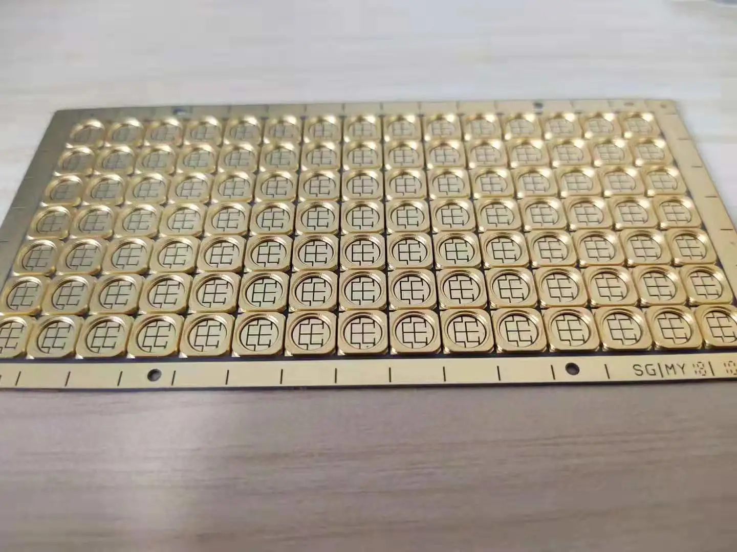
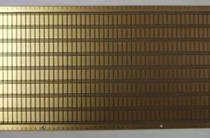
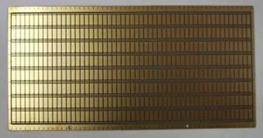
Metal Edged Ceramic PCB,Non Trace Metal Edging Ceramic PCB


Product Spotlights
Related Products
-
 China Chaosheng Electronics 3D Structured Alumina Ceramic PCB (3D Al ₂ O ∝ PCB) 3D Molding+multi-layer co FiringNegotiableMOQ: 1 Blade
 -
2-layer Aluminum Nitride Ceramic PCB,Single Layer Alumina 96% Ceramic PCB,NegotiableMOQ: 500 Units
-
1 Layer of 96% Alumina Ceramic PCB ,96% Aluminum Nitride Step Ceramic PCBNegotiableMOQ: 20000 Units
-
2-layer Monocrystalline Silicon Ceramic PCB,96% Aluminum Nitride Step Ceramic PCBNegotiableMOQ: 1 Blade
-
2 Layer of 96% Alumina Ceramic PCB,Concave Convex Alumina Ceramic PCBNegotiableMOQ: 1 Blade
If you have any needs, please feel free to contact China Chaosheng Electronics Company. Please contact us as follows:
whatsapp:+8613528819118
Skype live: pcb-fpcb88@163.com
E-mail : sales@chaoshengpcb-fpc.com
Contact: Mank. Li
Product areas: high-power equipment, High power server, high-power motor
Layers: 2-layer aluminum nitride ceramic thick copper ceramic PCB+embedded process ceramic PCB
Plate thickness: 1.60mm
Size: 120 * 59mm/1 * 1pieces
Process structure: Nitriding rate of 96%, copper thickness of 350um
Voltage withstand test: 100% short circuit test
The minimum mechanical hole is/mm, and the laser hole is/mm
Minimum line width and spacing of 20/20 mil
Surface treatment: Whole board electric gold, no solder mask
Features: heat dissipation, acid resistance, alkali resistance, corrosion resistance, anti-corrosion, etc
Usage: High temperature furnaces, transmission equipment, aviation, aerospace, high temperature furnaces, power systems, gas stations, power systems, electric furnaces and other products
Transport Package:Vacuum packaging+white paper insulation+moisture-proof beads+tin vacuum packaging+cardboard box
The ceramic board (ceramic PCB) technology of China Chaosheng Electronics (Shenzhen Chaosheng Electronic Technology Co., Ltd.) focuses on * * high thermal conductivity, high temperature resistance, and high reliability * *, targeting power electronics, RF LED、 High end scenarios such as automotive electronics cover four major areas: material systems, mainstream processes, precision manufacturing, and quality control.
1、 Core material system (determining the upper limit of performance)
Chaosheng Electronics mainly uses aluminum oxide and aluminum nitride, while also considering special ceramics such as silicon nitride, to meet different heat dissipation and strength requirements:
-Aluminum oxide (Al ₂ O3) * *: 96%/99% high-purity series, thermal conductivity * * 20-30 W/(m · K) * *, moderate cost, high insulation and voltage resistance, suitable for LED, industrial control, and consumer electronics power modules.
-Aluminum nitride (AlN): Thermal conductivity * * 170-220 W/(m · K) * *, thermal expansion coefficient close to silicon, suitable for high-power/high-frequency scenarios such as IGBT, MOSFET, 5G RF, etc.
-Silicon nitride (Si ∝ N ₄): with a bending strength greater than 600 MPa and excellent thermal shock resistance, it is suitable for strong vibration/large temperature difference environments such as automotive electric drives and photovoltaic inverters.
2、 Mainstream production processes (four major technical routes)
1. Direct bonding copper (DBC) - high-power main force
-Process: Ceramic substrate and copper foil are eutectic bonded at * * 1065-1085 ℃ * * to form an atomic level bonding interface.
-Advantages: Thick copper layer (* * 0.1-1.0 mm * *), strong current carrying capacity, long thermal cycle life, adhesion strength>* * 5 MPa * *.
-Application: New energy vehicle power module, IGBT module, industrial power supply.
2. Active Metal Brazing (AMB) - High end and Highly Reliable
-Process: Using Ag Cu Ti active brazing material, high-strength connection between ceramics and copper is achieved under vacuum/protective atmosphere at 800-900 ℃.
-Advantages: stronger adhesion, resistance to cold and hot impacts, and compatibility with advanced ceramics such as aluminum nitride/silicon nitride.
-Applications: Rail transit, aerospace, high-power lasers, medical equipment.
3. Direct Copper Plating (DPC) - Precision High Frequency
-Process: Sputtering Ti/Cu seed layer on ceramic surface → Photolithography pattern → Acidic copper plating thickening → Etching forming.
-Advantages: High line precision (line width/spacing * * 20-50 μ m * *), good flatness, suitable for high-frequency RF and COB packaging.
-Applications: 5G base station, optical communication, millimeter wave radar LED COB。
4. Thick film printing (TPC) - low-cost mass production
-Process: Screen printing silver/copper paste → drying at 150 ℃ → sintering at 850-900 ℃ to form a circuit.
-Advantages: Mature technology, low cost, suitable for medium and low precision, small and medium-sized batches.
-Applications: Sensors, thick film resistors, automotive electronic auxiliary circuits.
3、 Chaosheng's characteristic technology and process capability
1. * * High precision molding and surface treatment**
-Casting/dry pressing forming, thickness tolerance * * ± 5 μ m * *, flatness
-Support blind holes, buried holes, stepped grooves, and metalized holes to achieve three-dimensional interconnection.
-Surface treatment: immersion gold, thick gold (* * 1-200 μ "* *), nickel palladium plating to enhance oxidation resistance and welding reliability.
2. Multi layer ceramics and mixed pressing technology**
-Can be used for 2-8 layers of ceramic multilayer boards, suitable for high-density integration.
-Ceramic organic high-frequency mixed pressure, balancing heat dissipation and wiring density.
3. * * Customized special specifications**
-Ultra large/ultra-thin: maximum size * * 600 × 600 mm * *, thickness * * 0.2-3.0 mm * *.
-Thick copper: Copper thickness of * * 0.5-12 oz * * meets high current requirements.
-High thermal conductivity/high insulation: breakdown voltage>* * 20 kV/mm * *, suitable for high voltage scenarios.
###4、 Quality and reliability control
-System certification: * * UL, ISO9001, TS16949, ISO14000 * *, compliant with RoHS.
-Key tests: thermal resistance, thermal conductivity, adhesion, thermal shock (* * -55 ℃~150 ℃ * *, 1000 times), high temperature aging, insulation withstand voltage, ion pollution level.
-Equipment: imported precision casting machine, bonding furnace, sputtering/electroplating line, laser cutting machine, fully automatic detection equipment.
###5、 Typical application scenarios
-New energy vehicles: electric drive inverters OBC、DC/DC、BMS
-Industry and power supply: IGBT modules, photovoltaic inverters UPS、 laser power supply
-5G and RF: Base Station Amplifier, RF Module, Millimeter Wave Radar
-LED and Optoelectronics: COB Packaging, High Power Lighting, UV Curing
-Medical and Aerospace: Medical Imaging, Aerospace Electronics, Aerospace Power Supply

Send Inquiry to This Supplier

You May Also Like
-
2-layer 96% Aluminum Nitride Ceramic PCB,Concave Convex Alumina Ceramic PCBNegotiableMOQ: 1 Blade
-
2-layer Aluminum Nitride Ceramic PCBNegotiableMOQ: 500 Blades
-
2-layer Aluminum Nitride Ceramic Controlled Deep Step Ceramic PCBNegotiableMOQ: 500 Blades
-
2-layer Aluminum Nitride Ceramic Concave Step Ceramic PCBNegotiableMOQ: 1 Blade
-
2-layer Alumina Ceramic Thick Copper Ceramic PCBNegotiableMOQ: 1 Blade
-
2-layer Aluminum Nitride Ceramic Thick Copper Ceramic PCB+embedded Process Ceramic PCBNegotiableMOQ: 1 Blade
-
Multi Layer Coil PCB,Thick Copper Coil PCBNegotiableMOQ: 1 Blade
-
Multi-layer Flexible HDIFPC,High Pixel Nickel Palladium Gold Soft Hard Combination FPCNegotiableMOQ: 1 Blade
-
MiNiLEDPCB, Multi-layer MiNiLEDPCB, MiNiLEDHDIPCBNegotiableMOQ: 1 Blade
-
Hole Board Circuit Board PCB ,Dense Aperture 2.40 Hole Ultra Large Size PCB,Oversized Glass Screen PCBNegotiableMOQ: 1 Blade


