

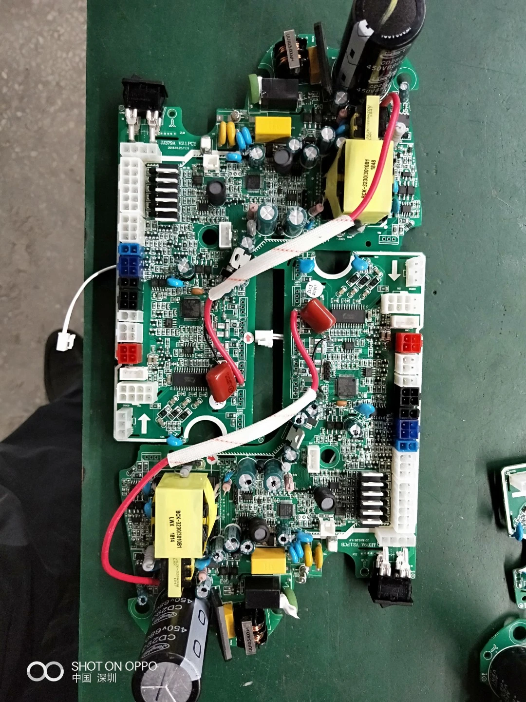
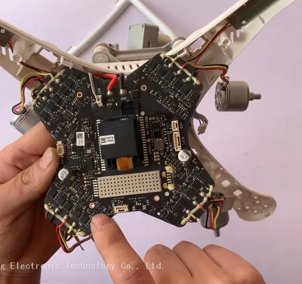
The Core of China Chaosheng Electronics' Drone PCB+PCBA


Product Spotlights
Related Products
-
 I Communication Server PCB+PCBA,backplane Server PCBANegotiableMOQ: 1 Blade
 -
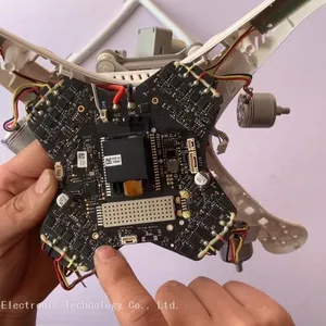
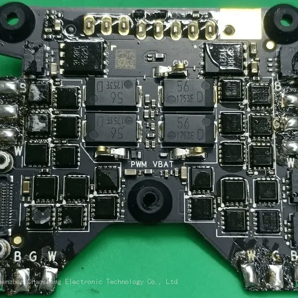
AI Power System PCB+PCBA,AI Drone Motherboard PCBANegotiableMOQ: 1 Blade
-
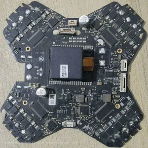
AI Autonomous Driving PCBA, Backplane Server PCBANegotiableMOQ: 1 Blade
-
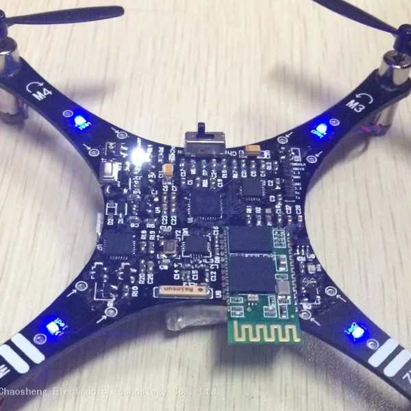
The Production Process of PCB+PCBA for AI Drone Driving by China Chaosheng Electronics is Centered AroundNegotiableMOQ: 1 Blade
-
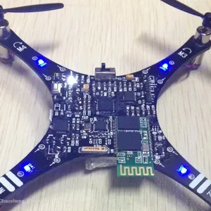
AI Drone Driving PCB+PCBA, AI Autonomous Driving PCBANegotiableMOQ: 1 Blade
If you have any needs, please feel free to contact China Chaosheng Electronics Company. Please contact us as follows:
whatsapp:+8613528819118
Skype live: pcb-fpcb88@163.com
E-mail : sales@chaoshengpcb-fpc.com
Contact: Mank. Li
The core of China Chaosheng Electronics' drone PCB+PCBA production process is to achieve stable and reliable flight control and signal transmission under five constraints: lightweight, high integration, strong anti vibration, excellent EMC, and good heat dissipation. Below are the key technologies for system disassembly from four dimensions: PCB design, PCB manufacturing, PCBA assembly, testing, and reliability.
1、 Core design technology of drone PCB
1. Stacking and structural design (determining performance limits)
Mainstream layers: consumer level 2-4 layers; Industrial/aerial photography 6-10 floors; High end flight control with 12+layers.
Standard stacking principle (6 layers as an example):
Top level: Signal (main control, IMU, sensors)
GND1: Complete ground plane (shielding, reflow)
Signal 2: High speed/differential (MIPI, SPI, UART)
PWR: Power plane (5V/3.3V/1.8V partition)
GND2: Complete Ground Plane
Bottom layer: signal (interface, power, low speed)
Key Design:
HDI high-density interconnect: blind/buried hole+micro hole (≤ 0.15mm), line width/spacing of 3-4mil, improves wiring density and reduces weight.
Rigid Flex: The preferred choice for folding/irregular structure drones, balancing rigid support and flexible wiring.
Hollow out weight reduction: Hollow out non critical areas, combined with ultra-thin core boards (0.2-0.4mm), can reduce weight by 10-30%.
2. Signal integrity (SI) and impedance control
Impedance matching:
RF/image transmission: 50 Ω single ended (microstrip/strip line).
High speed differential (MIPI, USB, Ethernet): 90-100 Ω differential, strictly equal length (error ≤ 5mil).
Clock/IMU bus: snake shaped with equal length to reduce phase difference.
Interference suppression:
Ground level isolation, 3W principle, differential tight coupling, short parallel segments.
Sensitive simulation (IMU, compass) and strong interference (ESC, motor drive) physical partitioning+shielding cover.
3. Power Integrity (PI) and EMC Design
Power architecture: Main power supply (12V/24V) → DC-DC (5V) → LDO (3.3V/1.8V analog), digital/analog ground single point common ground (magnetic beads/0 Ω).
Decoupling strategy:
Main control/BGA: 0402/0201 capacitor array (1 μ F+0.1 μ F+0.01 μ F), mounted next to the pins.
Electric tuning/power circuit: Thick copper (2-3oz)+high-capacity electrolytic/tantalum capacitors to reduce voltage drop and noise.
EMI/EMC:
Large area flooring, shielding cover, filtering (π - type/LC), common mode inductance of I/O ports.
Motor drive and flight control partition wiring to avoid high current loops cutting the ground plane.
4. Thermal management and anti vibration design
dissipate heat:
Thick copper+thermal via array is laid below the power devices (ESC, PMIC) to conduct heat to the bottom layer/chassis.
Aluminum/ceramic substrates are used for high-power electrical tuning, with a thermal conductivity of ≥ 2W/(m · K).
Anti vibration/anti impact:
Glue reinforcement at the four corners of large components (connectors, battery interfaces); Crystal oscillator/sensor encapsulation.
Add fixing holes and rubber washers at the edge of the board; Perform stress relief on key routing (rounded corners).
Select high Tg (≥ 170 ℃) and low CTE substrates to reduce delamination/cracking caused by temperature changes/vibrations.
5. Material selection (matching according to the scene)
table
Material Characteristics Applicable Scenarios
FR-4 (high Tg) cost-effective, flame retardant, stable mainstream consumer/industrial drones
Polyimide (PI) flexible, high temperature resistant (-200~260 ℃) rigid flex bonding, folding structure
Aluminum substrate with good thermal conductivity (1-4W), voltage resistant electrical adjustment, high-power LED
Rogers/high-frequency board low loss, stable Dk image transmission, WiFi, GPS RF
Ultra thin core board (0.2-0.4mm) ultra light, high-density micro/cross machine
Surface treatment: priority ENIG immersion gold (2 μ ''), good flatness, anti-oxidation, suitable for fine pitch BGA; OSP is used for low-cost consumer grade; The electrically regulated high current area can have locally thick gold/tin.
2、 Key processes for drone PCB manufacturing
1. Core process
LDI laser direct imaging: line width/line spacing accuracy ± 0.5mil, suitable for HDI fine wiring.
Vacuum lamination+step lamination: controls interlayer expansion and contraction, reduces misalignment and bubbles, suitable for 8-layer+high-density boards.
Micro hole/blind buried hole: laser drilling+electroplating filling to achieve high-density interconnection between layers.
Control deep milling/irregular machining: hollow out, step, half hole, suitable for structure and weight reduction needs.
2. Key control points
Copper thickness: signal layer 1oz; power/electrical control layer 2-3oz; hole copper ≥ 35 μ m, ensuring high current capability.
Impedance tolerance: ± 5% (RF/high-speed); ± 10% (normal signal).
Plate thickness tolerance: ± 0.05mm, ensuring assembly and flatness.
Reliability:
Thermal stress test: 288 ℃ float welding for 10 seconds without delamination or blistering.
Environmental adaptability: -40 ℃~+85 ℃ temperature cycle, damp heat, and salt spray meet the standards.
3、 UAV PCBA assembly process (mainly SMT)
1. Core process (double-sided reflow as the mainstream)
B-side (bottom layer): solder paste printing (SPI testing) → mounting (0201/01005 resistors, small connectors) → reflow soldering → adhesive fixation of large components (SD card slot, interface).
A-side (top layer): solder paste printing → mounting (main control, BGA, IMU, sensor) → reflow soldering.
Rear section: Wave soldering (plug-in) → Cleaning → Three proof coating → Board splitting → Testing.
2. Key process control
Mounting accuracy: ± 0.01~± 0.03mm, compatible with 01005 and 0.3mm BGA.
Reflow soldering: 10 temperature zone+nitrogen protection, precise temperature control curve to avoid B-side component detachment/remelting during secondary reflow.
Steel mesh design: laser cutting+electro polishing, stepped steel mesh with fine spacing areas, controlling tin content and reducing bridging.
Reinforcement process:
Large/heavy components: bottom glue+four corner reinforcement glue.
Connector/Interface: Selective wave soldering for secondary reinforcement to enhance vibration resistance.
Three proof paint (acrylic/polyurethane): moisture-proof, anti salt spray, anti mold, suitable for outdoor environments.
4、 PCBA testing and reliability verification
1. Process testing (full process quality control)
SPI: Solder paste thickness, offset, bridging screening.
AOI: Appearance of mounting/soldering (missing parts, offset, virtual soldering, soldering).
AXI (X-Ray): Internal solder joint voids, virtual soldering, and incomplete soldering in BGA/QFN (critical testing required).
ICT/flying pin testing: open circuit, short circuit, component error, resistance/capacitance screening.
2. Function and reliability testing (exclusive to drones)
FCT functional testing: Simulate flight conditions to verify the functions of flight control, sensors, communication, power supply, and motor drive.
Environmental Stress Screening (ESS):
Temperature cycle: -40 ℃~+85 ℃, 10-20 cycles.
Vibration: Three axis random vibration (5-2000Hz, 5-10 Grms), simulating flight impact.
Drop/Impact: Drop 1.5m, 1 time on each of the 6 sides.
EMC testing: Radiated/Conducted disturbances, immunity to ensure no interference with GPS/compass and compliance with regulations.
Long term aging: High temperature (60 ℃) charged aging for 48-168 hours, screening out early failures.
5、 Process differences among different types of drones
table
Type PCB Layer Core Process Reliability Requirements
Micro time travel machine with 2-4 layers of HDI, ultra-thin, hollowed out, lightweight (with priority given to drop resistance)
Consumer aerial photography of floors 4-6 with rigid scratching HDI、 Sinking gold, high EMC (stability+battery life)
Industrial/Plant Protection 6-8 layer thick copper and aluminum substrate, three proof, strong anti vibration, extremely high (24-hour operation)
High end/military 10-16 layer high-frequency materials, blind buried holes, redundant design top-level (extreme environment)
6、 Core Challenges and Solutions
Weight loss vs performance: HDI+ultra-thin+hollow out+micro components (01005), achieving ultimate weight loss while ensuring strength.
High density vs heat dissipation: thermal via array+thick copper+partitioned layout to avoid hotspot aggregation.
Strong vibration vs solder joint lifespan: adhesive reinforcement+optimized solder pad design+high reliability solder to enhance fatigue resistance.
Multiple interference sources vs. pure signal: partitioning+shielding+filtering+good grounding to ensure flight control and sensor stability.
7、 Summary
Drone PCB+PCBA is a system engineering of design, materials, manufacturing, assembly, and testing, with the core of finding the optimal balance between lightweight, compact, stable, strong, and long-lasting. From consumer level to industrial level, the complexity and reliability requirements of the process are gradually increasing, HDI、 Rigid scratch combination, precision SMT, and rigorous environmental testing are currently the mainstream technological directions.

Send Inquiry to This Supplier

You May Also Like
-
AI Unmanned Robot PCB+PCBA, AI Server PCB+PCBANegotiableMOQ: 1 Blade
-
AI Power System PCB+PCBA,backplane Server PCBANegotiableMOQ: 1 Blade
-
36 Layer Medical Product PCBA,60 Layer Communication Equipment PCBANegotiableMOQ: 1 Blade
-
8 Layers HDIPCBNegotiableMOQ: 1 Blade
-
16 Layer HDI Automotive Product PCBA,AI Communication Server PCBNegotiableMOQ: 1 Blade
-
42 Layers HDI Automotive Product PCBANegotiableMOQ: 1 Blade
-
48layer HDI Automotive Product PCBA,10 Layer HDI Arbitrary Order HDIPCBANegotiableMOQ: 1 Blade
-
10 Layers HDI Automotive Product PCBA,80 Layer Communication Server PCBANegotiableMOQ: 1 Blade
-
50layer HDI Automotive Product PCBA,18 Layer Intelligent Product PCBANegotiableMOQ: 1 Blade
-
AI Drone Driving PCB+PCBA,AI Communication Server PCB+PCBANegotiableMOQ: 1 Blade


