

MiNiLEDPCB, Multi-layer MiNiLEDPCB, MiNiLEDHDIPCB


Product Spotlights
Related Products
-
 P0.937MiLED8 Layer 3rd Order HDIPCB,MiNiLEDHDIPCBNegotiableMOQ: 1 Blade
 -
P0.925, INiLED8 Layer, 3rd Order HDIPCB,MiNiLEDHDIPCB,OMiNiLEDFPC,NegotiableMOQ: 1 Blade
-
P0.78 MiNiLED 8 Layers 2nd Order HDIPCB,MiNiLED Aluminum Based HDIPCB,MiNiLED Aluminum Based HDIPCBNegotiableMOQ: 1 Blade
-
P1.53MiNiLED4layer 1nd Order HDIPCBNegotiableMOQ: 1 Blade
-
P1.87MIPiLED6 Layer 2nd Order HDIPCBNegotiableMOQ: 1 Blade
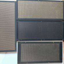
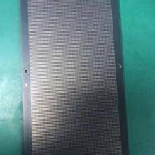
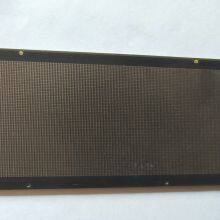
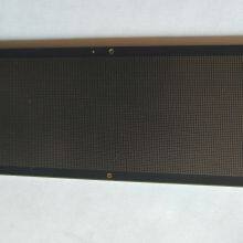
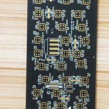
Product areas: MiNiLEDHDI, OMiNiLEDHDIPCB Layer number: P0.925, iNiLED8 layer, 3rd order HDIPCB Plate thickness: 3.0mm Size: 125 * 245mm/1 * 1 pcs Process structure: FR-4, TG150, resin plug hole, depth control, matte black Testing: Inner AOI 100% testing, Outer testing rack: 100% short-circuit testing The minimum mechanical hole is 0.15mm, the laser hole is 0.075mm, and the number of holes is
1.8 million, The minimum line width and spacing are 3/4mil Packaging method: vacuum packaging+separated white paper+cardboard box+cardboard board+air/sea freight Surface treatment: OSP, resin plug hole, depth control, matte black Features: PDA small, small spacing, laser drilling, with up to tens of thousands or even millions of holes, high cost, good lamp density effect. Usage: MiNiLED and OMiNiLED product series Main Product Structure of Chaosheng Group Company 2-80 layers of rigid circuit boards,
2-50 layers of flexible circuit boards and PCBA production Chaosheng Group Company mainly produces product categories High end double-sided, multi-layer, flexible, high-frequency, HDI interconnect, metal based, high thermal conductivity metal based, ceramic, cut in metal based, cut in buried capacitor, cut in thick copper buried magnet, concave convex step substrate,
5G high-speed board, thick copper, thick gold, high carbon resistance, double-sided multi-layer MiNi LED, MiNiHDILED, MiNiOLED, IC carrier substrate, roll to roll FPC, long FPC, large-sized printed circuit board, halogen -free material, high-frequency material, high-speed material, metal material, environmentally friendly circuit board, blind buried hole circuit board, high thermal conductivity aluminum based, thermoelectric separation copper based, PDU busbar, iron-based and metal based (core) mixed pressure plate, embedded copper buried copper. Buried resista nce buried capacitance buried ceramic bead board, ultra-thin BT board, ceramic substrate, IC carrier board, high-frequ ency mixed voltage, high-speed board, differential impedance board, thick copper plate, thick gold plated board,
HDI An integrated OEM and ODM production factory for Anylayer, double-sided, multi-layer, HDI FPC, soft hard c ombination HDI, roll to roll FPC, ultra long FPC, ultra large size PCB production and product design and development, software development, special material printed circuit boards, etc
| FAQ | |||
| Serial Number | Question Point | Answer | |
| Q1 | Q: What information is required to make a PCB | CEGSATE: Gberber files for PCB production, product process instructions, such as material requirements, surface treatment requirements, finished product thickness requirements, PCB stack structure diagram for advanced products, copper thickness requirements for each layer, sample quantity requirements, batch order requirements, product application fields, and other related information are required | |
| Q2 | Q: What information does PCBA need to provide | CEGSATE: BOM report is required (including the brand, specifications, and model of the components), X and Y coordinate numbers of PCBA components, and processing requirements: Do we need to purchase the components on our behalf? Or customer supplied components? Do you need software burning? What is the required quantity? What is the monthly demand and other detailed information. | |
| Q3 | Question: Is my file secure? | CEGSATE: Your files are very secure, and we protect intellectual property rights for our clients throughout the entire process. All files provided by the customer will never be shared with any third party. | |
| Q4 | Q: What is the minimum order quantity? | CESGATE: We do not have a minimum order quantity for PO orders. We are able to handle small and large batches flexibly. | |
| Q5 | Q: What is your inspection method? How do you control the quality? | CESGATE: In order to ensure the quality of PCB, FPC, and PCBA products, we use flying pin testing for small batches, which is usually used for samples and small batches; The inner circuit undergoes 100% optical inspection through AOI, and we have online AOI automatic inspection for intermediate inspection. Batch finished products undergo 100% inspection through E-SET testing rack. The appearance is 100% inspected by fully automated finished product testing equipment and FQC. PCBA undergoes automatic optical inspection (AOI), 100% X-ray inspection of BGA parts, and first article inspection (FAI). PCBA products that require software burning must undergo 100% comprehensive testing on the finished product testing rack according to product functional requirements before they can be shipped. |
|
| Q6 | Q: What standard should PCB be shipped according to? | WCESGATE: e accept and store according to the international IPC-6012 Level 2 standard. If there are special requirements for Level 3 standards in the quotation, we accept and store according to the international IPC-6012 Level 3 standardWe accept and store according to the international IPC-6012 Level 2 standard. If there are special requirements for Level 3 standards in the quotation, we accept and store according to the international IPC-6012 Level 3 standard | |
| Q7 | Q: May I ask how you package and ship? | 1:PCBVacuum packaging+separated white paper+moisture-proof beads+cardboard box 2:PCBVacuum packaging+white paper insulation+moisture-proof beads+tin vacuum packaging+cardboard box 3:PCBSpecial size PCB, vacuum packaging+separated white paper+moisture-proof beads+wooden frame or plastic bag packaging+separated white paper+moisture-proof beads+wooden frame 4: PCBA anti-static packaging 5: PCBA anti-static film+vacuum box packaging+shelving |
|
.

Send Inquiry to This Supplier


You May Also Like
-
P0.58,MiNiLED6 Layer, 2rd Order HDIPCB,MiNiLEDPCBNegotiableMOQ: 1 Blade
-
Hole Board Circuit Board PCB ,Dense Aperture 2.40 Hole Ultra Large Size PCB,Oversized Glass Screen PCBNegotiableMOQ: 1 Blade
-
AI Drone Driving PCB+PCBA,AI Communication Server PCB+PCBANegotiableMOQ: 1 Blade
-
AI Computing Power Server PCBANegotiableMOQ: 1 Blade
-
The Core of China Chaosheng Electronics' Drone PCB+PCBANegotiableMOQ: 1 Blade
-
I Communication Server PCB+PCBA,backplane Server PCBANegotiableMOQ: 1 Blade
-
AI Power System PCB+PCBA,AI Drone Motherboard PCBANegotiableMOQ: 1 Blade
-
AI Autonomous Driving PCBA, Backplane Server PCBANegotiableMOQ: 1 Blade
-
The Production Process of PCB+PCBA for AI Drone Driving by China Chaosheng Electronics is Centered AroundNegotiableMOQ: 1 Blade
-
AI Drone Driving PCB+PCBA, AI Autonomous Driving PCBANegotiableMOQ: 1 Blade


