

Home > Electrical & Electronics > Semiconductor > Intrinsic Semiconductor > High-purity Fused Silicon Wafer P-type N-type Crystal Direction of 100,110 for Scientific Research
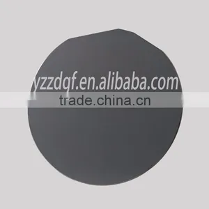
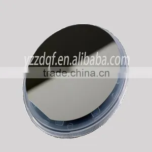
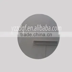
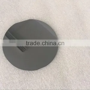
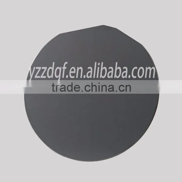
High-purity Fused Silicon Wafer P-type N-type Crystal Direction of 100,110 for Scientific Research


US$ 2 - 3
MOQ: 10 Pieces
Key Specifications
Get Latest Price
Place of Origin:
Jiangsu, China
Brand Name:
zhongding
Model Number:
P/N
Payment & Shipping
Payment Methods:
Port of Shipment:
Jiangsu
Delivery Detail:
Delivery time depends on order quantity.
Related Products
-
 Free Sample for Germanium Silicon Wafer for 2/3/4/5/6/8/12US$ 2 - 3MOQ: 25 Pieces
 -
High Purity P Type N Silicon Oxide Epitaxial Wafer High PurityUS$ 2 - 3MOQ: 10 Pieces
-
High Purity P Type N Square Silicon Wafer With High Purity of Crystal to 100 110US$ 2 - 3MOQ: 10 Pieces
-
8 Inches High-purity Silicon Oxide Wafer to 100.110 Thickness 650-725US$ 2 - 3MOQ: 10 Pieces
-
High Purity Alloy Silicon WafersUS$ 2 - 3MOQ: 10 Pieces
Place of Origin
Jiangsu, China
Brand Name
zhongding
Model Number
P/N
Product Description
Detailed Images
Tips
The company supports free to take samples of freight paid by the buyer
Company

Send Inquiry to This Supplier

Business Type
Manufacturer, Trading Company
Year Established
2009
Factory Size
1,000-3,000 square meters
Total Employees
11 - 50 People
You May Also Like
-
Intrinsic SemiconductorNegotiableMOQ: 2400 Pieces
-
New 12V 60W TEC1-12706 Thermoelectric Cooler Peltier Mini Thermoelectric Cooler and Warmer Thermoelectric Can CoolerUS$ 1 - 100MOQ: 100 Units
-
Temperature Indicator for Sputtering TargetUS$ 240 - 480MOQ: 10 Pieces
-
2012 NEW Scr Thyristor Module 200AUS$ 90 - 90MOQ: 1 Piece
-
CVD Boron Doped DiamondNegotiableMOQ: 10 Pieces
-
RENESAS R5F1026AASP#55 Microcontroller Microcontroller ConverterUS$ 1 - 500MOQ: 1 Bag
-
HEMT GaN On SiC For Power Wafer ManufacturersNegotiableMOQ: 15 Pieces
-
Control Unit Board H807ADPM H83DVCMM H807ADPE H831CCUC H835VDSHNegotiableMOQ: 1 Piece
-
Micro Porous Ceramic Suction Cup, Semiconductor Vacuum Suction Cup, Silicon Carbide Alumina Dense Ceramic Turntable Suction CupNegotiableMOQ: 100 Pieces
-
PFA 4inch Wafer Cassettes Etching Basket for SemiconductorNegotiableMOQ: 1 Piece


