

433.92mhz Wireless rf Receiver Module 1.2km Wireless Transmitter and Receiver Module


Related Products
-
 433.92mhz Wireless rf Receiver Module Cc1101 Wireless Module 1KM rf ModuleUS$ 4.5 - 5.4MOQ: 10 Pieces
 -
CC1110 433M Wireless Module rf Transceiver Module rf 433mhz ModuleUS$ 4.8 - 5.4MOQ: 10 Pieces
-
1km Wireless Transmitter and Receiver Module 470mhz Wireless Module CC1110 Soc8051US$ 5.5 - 6.9MOQ: 10 Pieces
-
5000m Transmit Long Distance RF Module UVA ApplicationUS$ 8.9 - 11.5MOQ: 10 Pieces
-
1km Wireless Transmitter and Receiver Module CC1110 rf Module With 8051 MCUUS$ 4.8 - 5.4MOQ: 10 Pieces
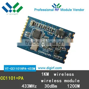
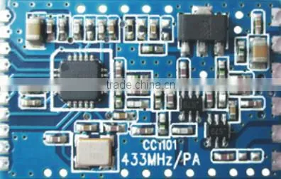
VT-CC1101HPA-433M Wireless Module User Guide
General Description
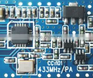
VT-CC1101HPA-433M is based on RF Transceiver CC1101 of TI Chipcon,it’s a small size and ultra low power UHF wireless module. CC1101 is a low cost true single chip UHF transmitter designed for very low power wireless applications. The circuit is mainly intended for the ISM (Industrial, Scientific and Medical) and SRD (Short Range Device) frequency bands at 315, 433, 868 and 915 MHz, The MAX RF output power can be set as high as +10dBm, with data rate as high as 500Kbps. The module integrated many RF functions and PA to make the maximum output power up to +30dBm. Customer can use it conveniently and reducing your development time.
Features
l Central frequency is 433MHz, Frequency bands :387~464MHz
l Programmable output power up to +30dBm for all supported frequencies,the communication distance is above 1200m in sight .
l High receiver sensitivity down to -112dBm(at 2.4Kbps data rate)
l Programmable baseband modulator with GFSK/2-FSK/ASK/OOK/MSK
l Programmable data rate 1.2~500Kbps
l 64-byte TX data FIFO
l Optional Forward Error Correction with Interleaving
l Support carrier sense and digital RSSI output
l Low current consumption with receive mode <22mA, transmit mode at +10dBm output power <250mA
l Low current consumption at power down state <2uA
l Wake-on-radio functionality for automatic low-power RX polling
l Integrated analog temperature sensor
l Efficient SPI interface, All registers can be programmed with one “burst” transfer
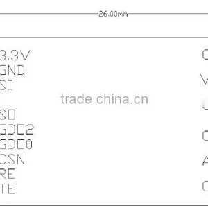
l Small dimension: 26.0mm×17.0mm×2.4 mm
l Operating supply voltage: 3.0~3.6V DC, PA supply voltage: 3.0~3.6V DC
Applications
l Logistics Tracking System, Warehouse patrol, Electronic label.
l Replace RS232 and RS485 in data transmission
l Industrial monitoring and control in data acquisition
l AMR – Automatic Meter Reading
l Home and building automation
l Consumer Electronics products of wireless control
l Wireless alarm and security systems
l Wireless sensor networks
General Characteristics
Test operating conditions:Ta=25°C,VCC=3.3V if nothing else stated.
Parameter |
Type |
Condition/Note |
Operating supply voltage |
DC 3.0~3.6V |
|
Central frequency |
433MHz |
Can be programmable to other frequency in bands 387~464MHz |
Frequency accuracy |
±10KHz |
|
Modulation format |
GFSK/2-FSK/ASK/OOK/MSK |
Programmable |
Transmit power |
-30~+30dBm |
Programmable |
TX current consumption |
<250mA |
Po=30dBm |
Receiver sensitivity |
-112dBm |
2.4Kbps |
RX current consumption |
<22mA |
2.4Kbps |
Sleep State current consumption |
<2uA |
Refer to IC operation states |
Data rate |
1.2~500Kbps |
Programmable |
Spurious emissions and harmonics |
< -30dBm |
TX power +10dBm. |
Communication distance |
>1200m |
Use VT-CC1101-433M as a receiver, 2-FSK modulation, 1.2kBaud data rata, +10dBm output power. |
Antenna impedance |
50ohm |
|
Operating temperature |
-20~+75 °C |
|
Storage temperature range |
-50~+125°C |
|
Dimension |
26.0 mm×17.0 mm×2.4mm |
See more in PCB description |
Note:
1. The module transmission data rate will affect Transmission distance ,the higher the data rate , the closer the distance, and the lower the receiving sensitivity.
2. The supply voltage to the module will affect TX power, in the operating supply voltage range, the lower the voltage, the lower the TX power.
3. The module central frequency will change as the operating temperature change, use it under suggest temperature, the module can work well.
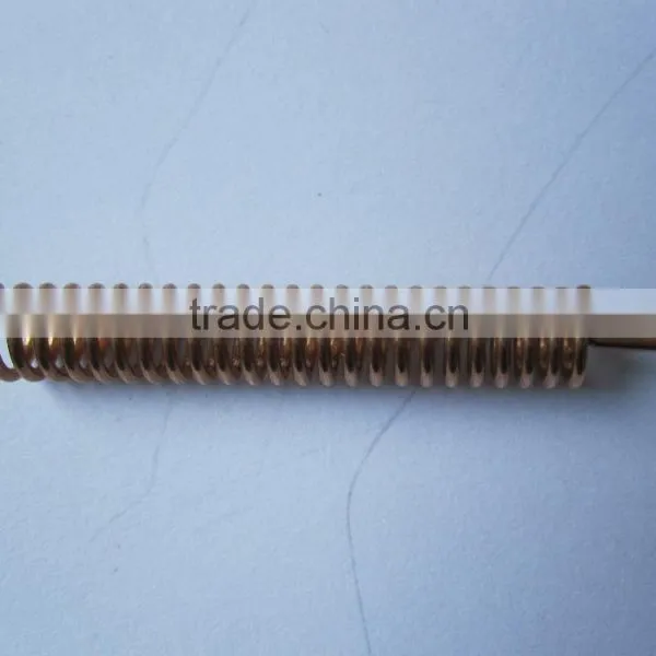
4. The antenna will strongly affect the communication distance, please select matched antenna and connect it correctly.
5. The module mount will affect the communication distance.
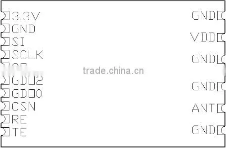
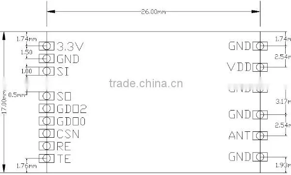
PCB Description
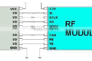
Pin Configuration
Pin name |
Pin type |
Description |
3.3V |
Power(Analog) |
1.8 V - 3.6 V analog power supply connection. |
GND |
Ground |
Connect to the system ground. |
SI |
Digital Input |
Serial configuration interface, data input. |
SCLK |
Digital Input |
Serial configuration interface, clock input. |
SO |
Digital Output |
Serial configuration interface, data output. Optional general output pin when CSN is high. |
GDO2 |
Digital I/O |
Programmable Clock output, down-divided from XOSC |
GDO0 |
Digital I/O |
Programmable Clock output, down-divided from XOSC. |
CSN |
Digital Input |
Serial configuration interface, chip select, active low. |
RE |
Digital Input |
RX state: RE=0(Low), TE=1(High) TX state: RE=1(High), TE=0(Low) |
TE |
Digital Input |
|
VDD |
Power(Analog) |
DC voltage from 3.0~9V input |
ANT |
RF I/O |
RF output signal from PA, connect to the Antenna. |
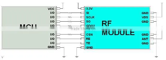
Circuit Interface
Note:
1. The module power supply voltage range is DC 3.0~3.6V, the PA supply voltage is DC 3.0~9.0V,above DC 3.6V, the module will damage. It is recommended work at DC 3.3 V, the PA supply voltage consider the application condition.
2. The module interface use half circle pad to soldering on the system PCB board, the GND must soldering to the system digital GND reliably.
3. The antenna must the get to the module’s ANT pin as close as possible.
4. The MCU which don’t have integrated SPI interface can also control the module, use the normal I/O port to work like SPI timing to read and write. The SPI data rate is below 10MHz.
5. The interface can connect directly to the MCU which use 3.3V power supply, there is no need serial resistor. If the I/O is open-drain, the pull-up resistor will be added. When connect to the MCU which use 5V power supply, the MCU’s I/O output current beyond 10 mA, a 2~5k ohm resistor will be series to divide the voltage, or it will damage the module.
6. The module’s pin GDO0 and GDO2 are general digital I/O ports, they can be programmable to produce trigger signal or clock output.
7. The PA control voltage have an effect on the communicate distance and power consumption. In transmit mode, set TE=0 and RE=1; in receive or sleep mode, set TE=1 and RE=0.
8. In the multiple channel application, the channel spacing is recommended to set as 1MHz, or there will be a same frequency interference.
9. The module TX power and current consumption reference to the PA supply voltage list in the table below:
VDD |
PO (dBm) |
(mA) |
3.0V |
21.63 |
97 |
3.6V |
22.98 |
111 |
4.5V |
24.61 |
132 |
5.0V |
25.34 |
142 |
6.0V |
26.52 |
161 |
7.0V |
27.33 |
176 |
7.5V |
28.11 |
185 |
9.0V |
28.71 |
204 |
10.
Operation States
CC1101’s operation states contain: Sleep State, Idle State, Active State,Sleep State is the lowest power mode. After wake up from Sleep State, the module get into Idle State. Except the Sleep State, each state can be switch by SPI interface, also programmed to auto-switch. CC1101’s radio control state diagram is shown as below, for detail information in the CC1101 datasheet.
Data Transmission
The CC1101 contains a 64 byte FIFO for data to be transmitted, built-in hardware support for packet oriented radio protocols, e.g. Preamble bytes, Synchronization Word, Whitening the data, CRC checksum, Interleave and Forward Error Code, Address checksum. The SPI interface is used for sending commend control and writing to the TX FIFO.
The format of the data packet can be configured and consists of the following figure:
In addition, CC1101 supports fixed packet length protocols, variable packet length protocols and infinite packet length. Details refer to the CC1101 datasheet.
Configuration Registers
The configuration of CC1101 can be done with software SmartRF Studio7. Complete descriptions of the registers are given in the CC1101 datasheet. We can provide evaluation board and demo code to the customer to develop and evaluate the module’s capability.
Dimension

Send Inquiry to This Supplier

You May Also Like
-
TYT Smarthome Gateway / Home Applainces Remote Comtroller in Zigbee Coordinator SystemUS$ 59 - 139MOQ: 1 Square Inch
-
Serial Wifi Module Wire Ethernet PCB Antenna Transparent Transmission WF-01US$ 1 - 10MOQ: 10 Pieces
-
External 3G Gsm Modem Pool 8 Port Speaker/call Sending Bulk SMS MMSUS$ 345 - 500MOQ: 1 Piece
-
RF DIN 7/16 Attenuator 50W 3dB/6dB/10dB/20dB/30dB/40dB/50dBNegotiableMOQ: 1 Piece
-
2015 New Stylish Optical Bluetooth Transmitter for Smartphone ,laptopUS$ 11 - 13MOQ: 1000 Pieces
-
UM220-III NUS$ 0.1 - 1MOQ: 1 Piece
-
2.4G WIFI/Bluetooth Internal FPC Antenna FR4 Antenna PCB Wifi Patch Antenna With IPEX UFL ConnectorUS$ 0.48 - 0.7MOQ: 100 Pieces
-
Bluetooth Audio Module RS232 Serial Bluetooth Module HC-06 Adapter Communication Master-Slave 2 Modes MINI USBUS$ 1 - 100MOQ: 100 Units
-
RIGHT ANGLE f QUICK MALE RF CONNECTORUS$ 0.01 - 0.99MOQ: 1000 Pieces
-
High Strength FRP RadomeNegotiableMOQ: 100 Pieces


