

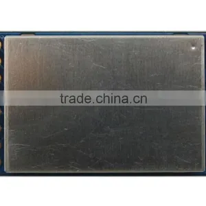
Cc1120 PA Anti Noise Cancel LNA 433.92mhz Wireless rf Receiver Module
Related Products
-
 Wireless Temperature Sensor 433mhz Module CC1110 rf Module SOC 8051 MCUUS$ 4.8 - 5.4MOQ: 10 Pieces
 -
rf 433mhz Weather Station Module Long Distance TransmitUS$ 5.4 - 6.2MOQ: 10 Pieces
-
Wireless 1km rf Module Cc2500 2.4ghz rf Module Cc2500US$ 4.6 - 5.5MOQ: 10 Pieces
-
2.4g Wireless Receiver Cc2500 Module With AntennaUS$ 4.5 - 5.4MOQ: 10 Pieces
-
Cc1101 rf Module 433mhz rf Module Wireless ModuleUS$ 2.5 - 3MOQ: 10 Pieces
General Description
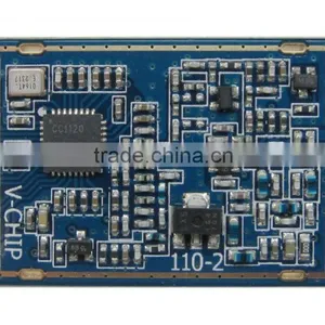
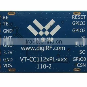
VT-CC1120PL-433M is based on RF Transceiver CC1120 of TI Chipcon,CC1120 is fully integrated single-chip radio transceiver designed for high performance at very low power and low voltage operation in cost effective wireless systems. Added PA, LNA circuit, enhanced output power and sensitivity.The module integrated many RF functions thus you can use it conveniently and reducing your development time.
Features
433MHz wireless transceiver, Frequency bands at 169M/868M/915M/950MHz be customized
Programmable baseband modulator with 2-FSK, 2-GFSK, 4-FSK,4-GFSK,MSK,OOK/ASK
3.3V , max power +26 dBm
Transmit distance reached 5000 meters, and sensitivity reached -125dBm when setting is 1.2kbps, DEV=4KHz, RX BW=25KHz
Powerful signal processor, deal with strong signal very clear.
Programmable data rate to 200Kbps
Low power consumption and operating supply voltage:2.0~3.6V DC
Point to point and point to multi-point communication.
Support carrier wave and digital RSSI output.
Separate 128-byte RX and TX FIFOs
High stability and industrial reliability
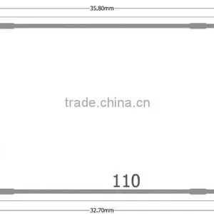
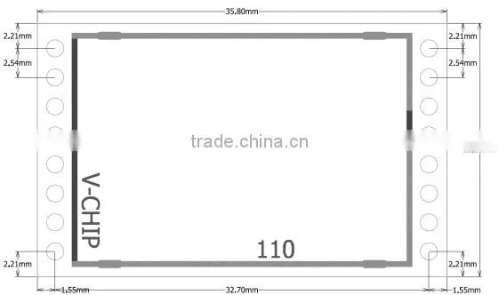
Small dimension:23.05mm×15.06mm×1.8 mm
Applications
Wireless Metering and Wireless Smart Grid (AMR and AMI)
Logistics Tracking System, Warehouse patrol, Electronic label
Industrial monitoring and control
AMR – Automatic Meter Reading
Home and building automation
Consumer Electronics products of wireless control
Wireless alarm and security systems
Wireless sensor networks
General Characteristics
Test operating conditions:Ta=25°C,VCC=3.3V if nothing else stated.
Parameter Type Condition/Note
Operating supply voltage DC 2.0~3.6V
Frequency range 410-480MHz Programmable
Frequency accuracy ±10ppm
Modulation format 2-FSK/4-FSK/2-GFSK/4-FSK/MSK/OOK Programmable
Transmit power MAX:26dBm(3.3V) Programmable
TX current consumption ≤250mA
Receiver sensitivity -125dBm(1.2kbps DEV=4KHz RX BW=25KHz) Refer to data rate
RX current consumption ≤25mA
Sleep State current consumption <1uA
Transmit distance 5000M
Antenna impedance 50ohm
Operating voltage 3.0~3.6V
Operating temperature -20~+75 °C
Storage temperature range -40~+125°C
Dimension 23.05mm×15.06mm×1.8 mm See more in PCB description
Note:
1.The module transmission data rate will affect Transmission distance ,the higher the data rate , the closer the distance, and the lower the receiving sensitivity.
2.The supply voltage to the module will affect TX power, in the operating supply voltage range, the lower the voltage, the lower the TX power.
3.The module central frequency will change as the operating temperature change, use it under suggest temperature, the module can work well.
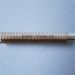
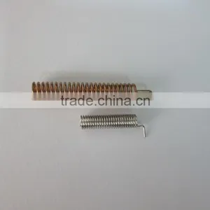
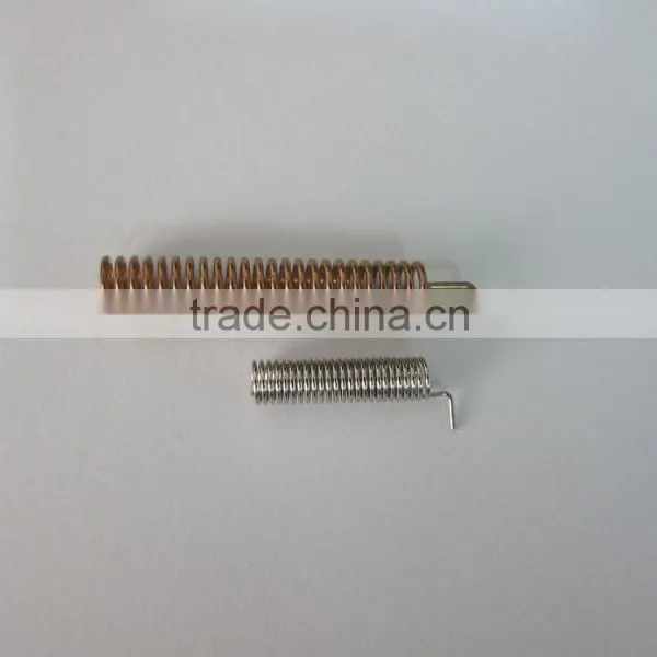
4.The antenna will strongly affect the communication distance, please select matched antenna and connect it correctly.
5.The module mount will affect the communication distance.
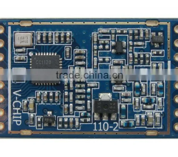
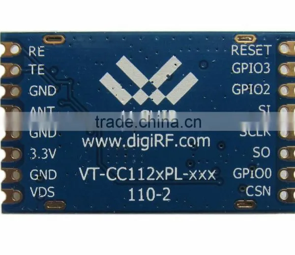
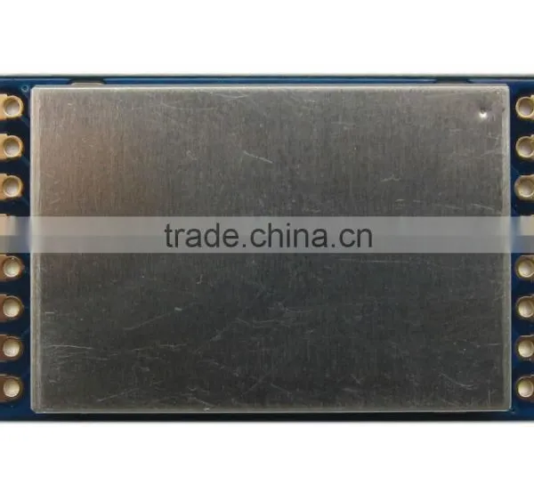
PCB Description
Pin Configuration
Pin name Pin type Description
RESET_N Digital in Reset; low level valid
GDIO3 Digital in/out Digital I/O, register configuration
GDIO2 Digital in/out Digital I/O, register configuration
SI Digital In Digital in (SPI)
SCLK Digital In Time input (SPI)
SO/GPIO1 Digital In/out Digital output (SPI) or general digital In/out port
GDIO0 Digital In/out Digital I/O, register configuration
CSN Digital I/O Module select (SPI), low level valid
RE Status control RX=0,TX=1,SLEEP=0
TE Status control RX=1,TX=0,SLEEP=0
GND ground
ANT Antenna port Impedance 50 ohm
3.3V Work power DC 3.0-3.6V
VDS Power amplifier Power amplifier, default short circuit
Circuit Interface
Note:
The pin sequence above are not the actual pin sequence refer pin description. SPI, I/O interface should connect with the MCU’s I/O pin in order to archive your functions. The circuit must be take ESD protect to prevent damage module. Good RF performance determines on the module position, ground and antenna fixing. Any question about the module please contact with the FAE engineer.
Configuration Registers
The configuration of CC1120 can be done with software SmartRF Studio7. Complete descriptions of the registers are given in the CC1120 datasheet. We can provide evaluation board and demo code to the customer to develop and evaluate the module’s capability.

Send Inquiry to This Supplier

You May Also Like
-
TYT Smarthome Gateway / Home Applainces Remote Comtroller in Zigbee Coordinator SystemUS$ 59 - 139MOQ: 1 Square Inch
-
Serial Wifi Module Wire Ethernet PCB Antenna Transparent Transmission WF-01US$ 1 - 10MOQ: 10 Pieces
-
External 3G Gsm Modem Pool 8 Port Speaker/call Sending Bulk SMS MMSUS$ 345 - 500MOQ: 1 Piece
-
RF DIN 7/16 Attenuator 50W 3dB/6dB/10dB/20dB/30dB/40dB/50dBNegotiableMOQ: 1 Piece
-
2015 New Stylish Optical Bluetooth Transmitter for Smartphone ,laptopUS$ 11 - 13MOQ: 1000 Pieces
-
UM220-III NUS$ 0.1 - 1MOQ: 1 Piece
-
2.4G WIFI/Bluetooth Internal FPC Antenna FR4 Antenna PCB Wifi Patch Antenna With IPEX UFL ConnectorUS$ 0.48 - 0.7MOQ: 100 Pieces
-
Bluetooth Audio Module RS232 Serial Bluetooth Module HC-06 Adapter Communication Master-Slave 2 Modes MINI USBUS$ 1 - 100MOQ: 100 Units
-
RIGHT ANGLE f QUICK MALE RF CONNECTORUS$ 0.01 - 0.99MOQ: 1000 Pieces
-
High Strength FRP RadomeNegotiableMOQ: 100 Pieces


