








 Contact Platform Support
 Help Center
China Chaosheng Electronics | Complete Production Technology for Automotive, Medical, 5G Communication, Radar, Antenna, and Server Control Board PCB
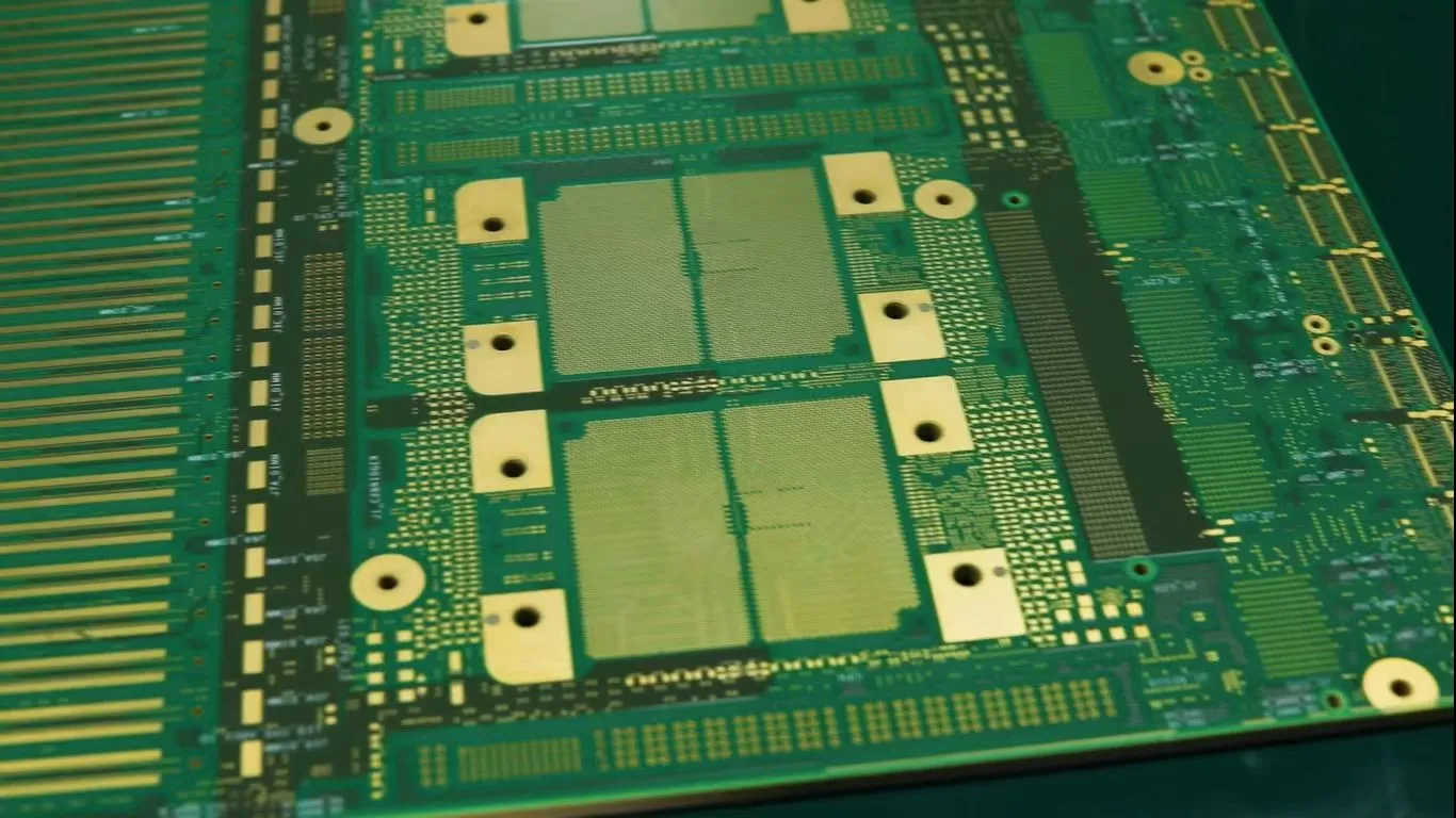
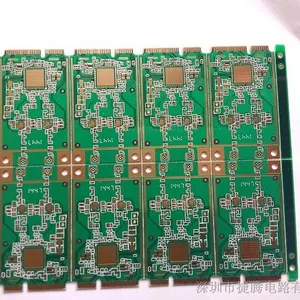
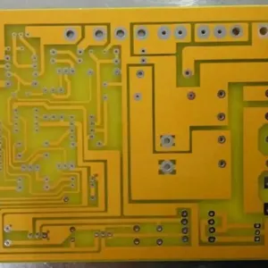
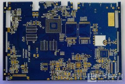
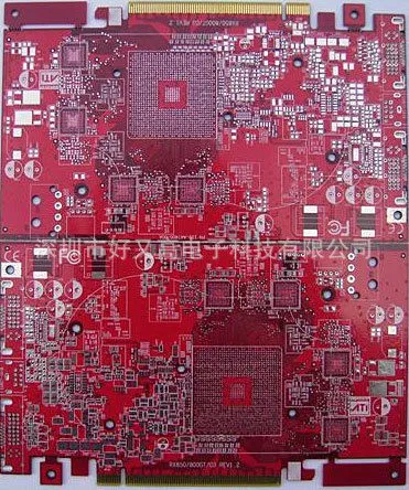
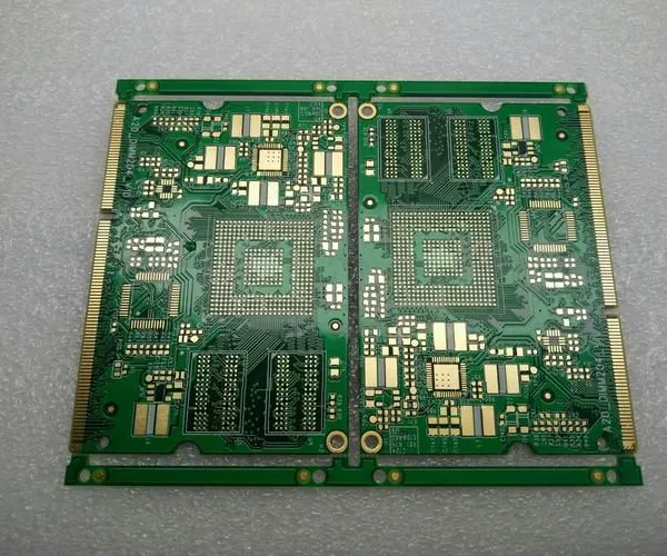
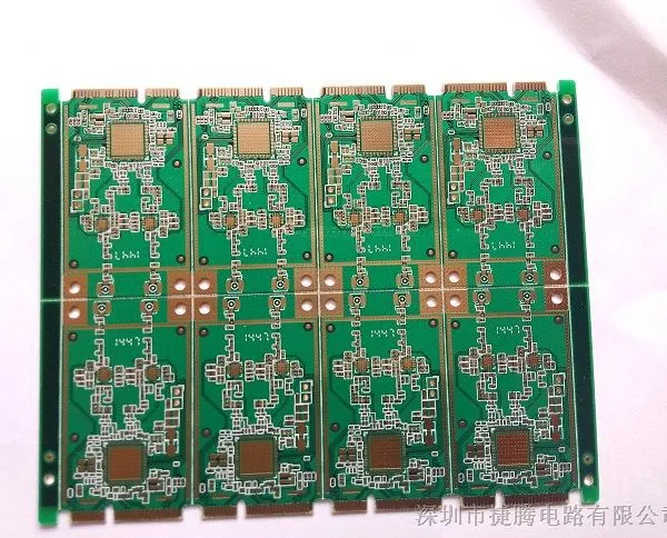
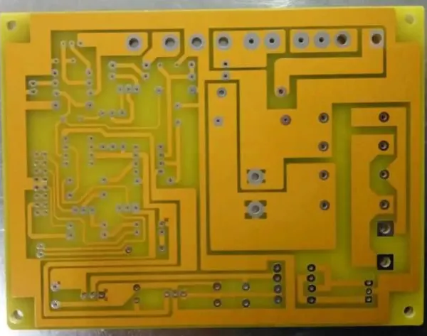
Product Spotlights


Related Products
-
 China Chaosheng Electronics | High Frequency and High-speed 5G Communication, Radar, Antenna, Server Main Control Board PCBNegotiableMOQ: 1 Blade
 -
China Chaosheng Electronics | 80 Layer High-frequency and High-speed 5G Communication, Radar, Antenna, Server Main Control Board PCBNegotiableMOQ: 1 Blade
-
China Chaosheng Electronics | 80 Layer AI Server Main Control Board PCB Complete Production Technology and ApplicationNegotiableMOQ: 1 Blade
-
China Chaosheng Electronics | Power System Motor, 5G Communication, Radar, Antenna, Server Main Control Board PCBNegotiableMOQ: 1 Blade
-
China Chaosheng Electronics | Power Drive System Motor PCB Server Main Control Board PCB,Thick Hard Gold Finger Circuit Board,Radar RF Microwave PCB,NegotiableMOQ: 1 Blade
China Chaosheng Electronics | Complete Production Technology for Automotive, Medical, 5G Communication, Radar, Antenna, and Server Control Board PCB
Automotive electronics PCB, Medical equipment circuit board, Industrial control PCB, Aerospace & military grade PCB, Ion‑equipment high‑voltage board, High‑speed server PCB, 5G communication circuit board, Radar RF microwave PCB, Wireless terminal motherboard, Industrial SBC mainboard, High‑power industrial control PCB, Automation controller board, Drone flight‑control PCB, Robot control board, High frequency low loss PCB, Thick hard gold finger circuit board, HDI blind & buried via PCB
1、 Overview of Overall Process Capability
Can be used for * * 2-80 layers * * precision circuit boards, covering rigid PCBs, FPC soft boards, soft hard bonding boards, high-frequency and high-speed boards, BT boards, metal substrates (aluminum based/thermoelectric separation copper based), buried resistors and capacitors, arbitrary order HDI, ultra large and ultra long boards, roll to roll FPC, supporting PCBA-SMT one-stop processing, with * * IATF16949 automotive, ISO13485 medical UL、 High frequency RF, high reliability server * * process system.
2、 Automotive electronic PCB (autonomous driving, onboard control, radar, body, battery management BMS)
Core board
High speed FR-4, low loss high-frequency material, metal thermal conductive substrate, BT board, high Tg halogen-free material
Key technical indicators
1. Layers: 2-36 layers; Line width and spacing * * 35 μ m * *; Micro hole 0.075mm laser blind hole
2. Impedance control: differential 100 Ω± 5%, single ended 50 Ω± 8% (millimeter wave radar hard index)
3. Copper thickness: 0.5~8OZ, BMS high current area can achieve 12OZ thick copper, embedded buried copper strip
4. Surface treatment: ENIG immersion gold, ENEPIG nickel palladium gold (priority, vibration resistance, high and low temperature resistance, can be repaired multiple times), ordinary tin spraying is prohibited for use in car safety components
5. Reliability Process
-Temperature cycle: -40 ℃~+125 ℃, 1000 times without stratification
-Salt spray 48-96H, CAF ion migration suppression, anti vibration, low warpage ≤ 0.3%
-IATF16949 full process traceability, AOI+AXI+electrical testing 100% full inspection
Typical products
77G/24G millimeter wave radar board, laser radar main control board, autonomous driving domain controller board, onboard central control, BMS power board, onboard antenna PCB
3、 Medical equipment PCB (imaging equipment, monitoring, analyzer, minimally invasive surgical instruments)
Plate selection
High reliability FR4, low Df high-frequency substrate, ultra-thin soft hard bonding FPC, ceramic substrate
Key points of process
1. Layers: 2-40 layers; Fine circuit 25 μ m; Blind buried hole HDI
2. Low ion precipitation, high insulation withstand voltage, CAF suppression process to prevent leakage interference with precision sensors
3. Surface treatment: Sinking gold/nickel palladium gold, gold thickness of 0.05-0.2 μ m, stable solder joints, capable of multiple high-temperature disinfection welding
4. Biocompatible process control, production workshop cleanliness level, can meet ISO13485 system requirements
5. Accurate impedance, suitable for weak signal transmission in ultrasound and MRI signal acquisition boards
Finished Product Inspection
Insulation withstand voltage test, high and low temperature aging, impedance TDR full sampling test, 3D-AOI optical detection
Typical Applications
Ultrasound imaging motherboard, monitor control board, endoscope soft hard combination board, medical testing instrument main control board
4、 5G/Communication, Antenna, Radar RF PCB Technology
substrate
Rogers、 Taikangni, Shengyi high-frequency high-speed board, high-frequency mixed pressure structure, PTFE mixed pressure plate, ultra-thin HDI, antenna specific FPC soft board
RF key parameters
1. The dielectric constant DK tolerance is ± 0.05, and the loss factor Df is extremely low
2. Differential impedance ± 3%~5%, single ended 50 Ω strictly controlled, line width compensation, copper foil roughness control
3. Laser micro hole 0.08-0.15mm, reducing via signal loss
4. Multi layer hybrid (high-frequency layer+ordinary FR-4 composite), controlling costs while ensuring RF performance
5. Ultra thin process for antenna board: board thickness of 0.12-0.4mm; batch production capacity for roll to roll FPC antenna
6. The radar board has a multi-layer shielding structure, with an inner grounding shielding layer to reduce crosstalk and prevent electromagnetic interference
Applicable Products
5G base station motherboard, RF unit RRU, millimeter wave radar, satellite communication board, built-in antenna PCB, wireless terminal RF board
5、 AI server, computing power control circuit board
Core technology direction: High multilayer, ultra-high current, high heat dissipation, high-density interconnection HDI/Any Layer blind buried hole of any order
1. Layers: 8-60 layers; Interlayer alignment accuracy ± 25 μ m
2. High current power supply scheme: 2-8OZ thick copper, embedded copper blocks, large-area power supply layer, voltage drop deviation ≤ ± 5%
3. High density wiring: LDI laser imaging, minimum L/S 25/25 μ m
4. Heat dissipation process
-High density thermal conductive plug hole (filled with resin and thermal conductive slurry)
-Heat dissipation via array, vertical thermal conduction channel
-Optional thermoelectric separation copper based for high-power power supply areas
5. High speed signal substrate: BT board, high-speed low loss copper-clad laminate, supporting 25Gbps to 112Gbps signal transmission
6. Surface technology: ENEPIG nickel palladium gold, resistant to multiple reflow soldering, suitable for BGA and large package chips
7. Backboard ultra large size process: The maximum board size is * * 1000 * 560mm * *, which meets the requirements of server backboards
6、 Our own unique and differentiated technology (with universal advantages across multiple industries)
1. * * Any level HDI cross blind buried hole Any Layer * *, suitable for high-density vehicles, servers, and medical boards
2. Buried resistance, buried capacitance, embedded copper * *, reduce board area, lower parasitic parameters, high-frequency noise reduction
3. Thermal electric separation copper/aluminum substrate * *, high-power, radar power amplifier, power module heat dissipation solution
4. Rigid Flex * *: 2-26 layers, suitable for medical probes and car folding antennas
5. * * Roll to roll R2R FPC * *, long flexible antenna, light strip module, micro sensor
6. * * Extra long and ultra large size PCB * *, solving the size limitations of server backboards and industrial control large screen boards
7、 Complete production process
Engineering data review → DFM manufacturability analysis → inner layer graphics → AOI → lamination → laser/mechanical drilling → copper plating → outer layer LDI imaging → etching → solder mask characters → surface treatment → outer edge → flying pin/ICT electrical testing → 3D-AOI → reliability testing → FQC shipment, expandable SMT PCBA one-stop service

Send Inquiry to This Supplier


You May Also Like
-
AI Autonomous Driving PCB,China Chaosheng Electronics | AI Server Main Control Board PCBNegotiableMOQ: 1 Blade
-
5G Communication Circuit BoardPCB,China Chaosheng Electronics | Complete Production Technology and Application of ComputingNegotiableMOQ: 1 Blade
-
Roll-to-Roll R2R Flexible PCB,800G Optical Module R2R FPC,NegotiableMOQ: 1 Blade
-
2-layer Alumina 96% Ceramic PCB,Double Layer Oxidized 96% Aluminum Ceramic PCBNegotiableMOQ: 500 Units
-
8LayersHDIPCB,HDI High-frequency High-speed Material PCBNegotiableMOQ: 10 Blades
-
16 Layer Multi-layer Circuit Board PCB,HDI Ultra-thin PCBNegotiableMOQ: 1 Blade
-
16 Layer Multi-layer Circuit Board PCB,HDI Ultra Large PCBNegotiableMOQ: 20 Blades
-
10 Layers, 3rd Order Multi-layer Circuit Board PCB,double-layer Ultra Large PCBNegotiableMOQ: 10 Blades
-
28 Layers, 3rd Order Multi-layer Circuit Board PCB,Double Layer Ultra-thin PCBNegotiableMOQ: 1 Blade
-
52 Layers, 3rd Order Multi-layer Circuit Board PCBNegotiableMOQ: 1 Blade


