

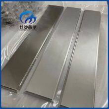
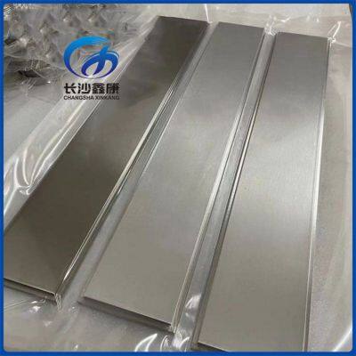
Factory Supply Nickel Chromium Sputtering Target NiCr Alloy Target NiCr20 NiV80/20wt% for PVD Coating


Related Products
-
 Nickel Copper (NiCu) Sputtering Target Customize Size for PVD CoatingUS$ 85 - 125MOQ: 1 Piece
 -
Nickel Iron Alloy Target NiFe Alloy NiFe20wt% NiFe90/10wt% Sputtering TargetsUS$ 85 - 255MOQ: 1 Unit
-
Xinkang Produce Nickel Vanadium Alloy Target NiV Alloy NiV7 NiV93/7wt% Sputtering TargetsUS$ 100 - 185MOQ: 1 Piece
-
Factory Supply Nickel Vanadium Sputtering Target NiV Alloy Target NiV7 NiV93/7wt% for PVD CoatingUS$ 85 - 185MOQ: 1 Piece
-
XinKang Chromium Targets 99.95% Purity Cr Chromium Sputtering Targets Customize SizeUS$ 55 - 185MOQ: 1 Piece
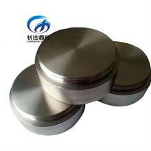
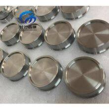
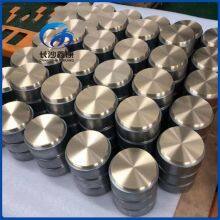
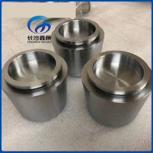
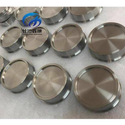
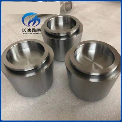
Nickel Chromium (NiCr) Sputtering Target
| Attributes Name | High purity metal alloy sputtering target |
| Product Name | NiCr Sputtering Target |
| Element Symbol | Ni+Cr |
| Purity | 3N, 3N5 |
| Shape | Planar |
Preparation process of nickel-vanadium alloy sputtering target
Material Preparation - Vacuum Induction Melting - Chemical Analysis - Forging - Rolling - Annealing - Metallographic Inspection - Machining - Dimensional Inspection - Cleaning - Final Inspection - Packaging
In the fabrication of integrated circuits, pure gold is generally used as interconnect metal, deposited on a silicon wafer, but gold will diffuse into the silicon wafer to form a high-resistance AuSi compound, which will greatly reduce the current density in the wiring, resulting in the failure of entire wiring system.
So, It is proposed to add adhesive layer between the gold thin film and silicon wafers. The adhesive layer is usually made of pure nickel, but diffusion also occurs between the nickel layer and the gold conductive layer, so that a barrier layer is needed to prevent diffusion between the gold conductive layer and nickel adhesive layer.
With a high melting point and a large current density, vanadium is chosen to deposit barrier layer, therefore, nickel sputtering target, vanadium sputtering target, gold sputtering target are all used in the fabrication of integrated circuits.
Nickel vanadium NiV sputtering targets containing 7% vanadium has both advantages of nickel and vanadium, thus adhesive layer and barrier layer can be achieved at a time. NiV alloy is non-magnetic materials, which is conducive to magnetron sputtering. In the electronics information industry, it is gradually replacing pure nickel sputtering targets.
The picture below are two micrographs of our NiV(93/7 wt%) alloy sputtering target, the average grain size<100μm.

Send Inquiry to This Supplier

You May Also Like
-
XinKang Cobalt Targets 99.95% Purity Co Cobalt Sputtering Targets Customize SizeUS$ 55 - 125MOQ: 1 Piece
-
99.95% Ni Nickel Pellets D3x3mm 1-10mm Metal Nickel Granules for Nickel Evaporation MaterialsUS$ 75 - 125MOQ: 1 Kilogram
-
99.99% Purity Nickel Pellets D3x3mm D6x6mm Nickel Granules Evaporation MaterialsUS$ 55 - 135MOQ: 1 Kilogram
-
Tantalum Pellets 99.95% Purity Metal Ta Tantalum Evaporation Materials Ta GranulesUS$ 85 - 165MOQ: 1 Gram
-
Tantalum Plate Targets 99.95% Ta Tantalum Targets Plate Sheet for PVD CoatingUS$ 85 - 200MOQ: 1 Piece
-
Iridium Sputtering Targets 99.95% Pure Ir Iridium Disc Targets for Thin Film CoatingNegotiableMOQ: 1 Piece
-
Aluminum Sputtering Targets 99.99% Al Aluminum Targets for PVD CoatingNegotiableMOQ: 1 Piece
-
Indium Foil 99.995% Purity 0.1x100x100mm In Indium Foil Customize SizeNegotiableMOQ: 1 Piece
-
Indium Wire 99.995%-99.9999% Purity Diameter 1mm 1.5mm In Indium Wire Customize SizeNegotiableMOQ: 1 Roll
-
Rhenium Target 99.95% Purity Re Rhenium Sputtering Targets Customize SizeNegotiableMOQ: 1 Piece


