

Home > Electrical & Electronics > Electrical Control System > TOKYO ELECTRON TEB207-12 OGSI EC80-000157-12 Electronic Module
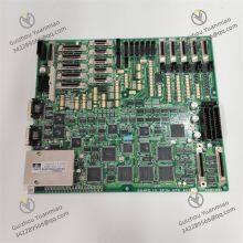
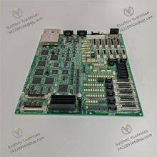
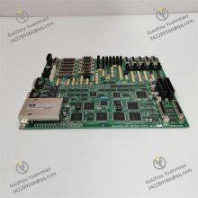
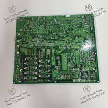
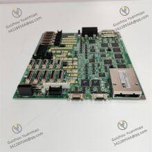
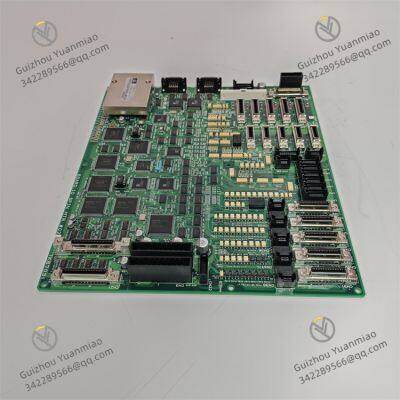
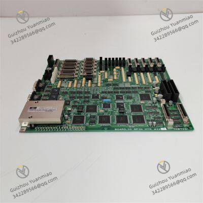
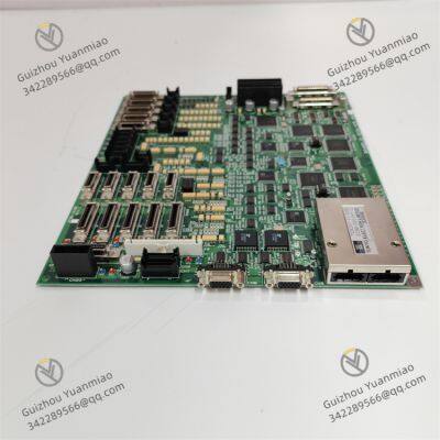
TOKYO ELECTRON TEB207-12 OGSI EC80-000157-12 Electronic Module


Negotiable
MOQ: 1 Piece (Price negotiable depending on order volume and customization)
Key Specifications
Get Latest Price
Material:
Other, Global universal model
Condition:
Other, Global universal model
Task:
Other, Global universal model
Payment & Shipping
Payment Methods:
Port of Shipment:
guizhou
Delivery Detail:
Delivery time depends on order quantity.
Related Products
-
 Eaton CS-TX3-3. 81X2.54-64TW Pluggable Terminal BlockNegotiableMOQ: 1 Piece
 -
REXROTH VT-HNC100-1-23/M-08-P-0 Digital Axis ControlNegotiableMOQ: 1 Piece
-
DEIF PSM-1 Power Supply ModuleNegotiableMOQ: 1 Piece
-
DEIF CM-2 Control ModuleNegotiableMOQ: 1 Piece
-
DEIF IPM-1 Intelligent Power ManagerNegotiableMOQ: 1 Piece
Material
Other, Global universal model
Condition
Other, Global universal model
Task
Other, Global universal model
Mathematical Model
Other, Global universal model
Signal
Other, Global universal model
Customized
Non-Customized
Structure
Other, Global universal model
Operating Temperature
20℃~28℃
Relative Humidity
30%~60% (non-condensing)
Storage Temperature
-40℃~85℃
Dimensions
150mm×100mm×40mm
I. Overview
II. Technical Parameters
1. I/O Channel and Signal Parameters
2. Control Performance Parameters
3. Environmental and Reliability Parameters
III. Functional Features
1. Precise Process Parameter Control for Advanced Etching/Deposition Processes
2. Strong Plasma/Electromagnetic Interference Protection for Harsh Process Environments
3. High Reliability and Safety Design for Uninterrupted Mass Production
4. Exclusive Adaptation to TEL Equipment for System Synergy

Send Inquiry to This Supplier

* Email
Want the best price?
Post an RFQ now!

1Yr
Business Type
Trading Company
Year Established
2014
Factory Size
1,000-3,000 square meters
Product Certifications
SA8000
You May Also Like
-
DEIF OPM-1 A Versatile Operator PaneNegotiableMOQ: 1 Piece
-
DEIF SCM-1 Microprocessor-Based Synchronization Control ModuleNegotiableMOQ: 1 Piece
-
PROVIBTECH TM201-A02-B00-C00-D00-E00-G00 Vibration TransmitterNegotiableMOQ: 1 Piece
-
PROVIBTECH TM201-A00-B00-C00-D00-E00-G00 Vibration ProtectionNegotiableMOQ: 1 Piece
-
PROVIBTECH TM202-A00-B00-C00-D00-E00-G00 Vibration TransmissionNegotiableMOQ: 1 Piece
-
PROVIBTECH TM521-A02-B00-C02-D00-E01-G00-10-M1 Vibration Monitoring ModuleNegotiableMOQ: 1 Piece
-
PROVIBTECH TM501-A03-B00-C00-D00-F00-G00 Vibration Monitoring ModuleNegotiableMOQ: 1 Piece
-
PROVIBTECH TM591-B00-G00 Eddy Current Vibration ProbeNegotiableMOQ: 1 Piece
-
CUTLER HAMMER 1755T-PMPP-1700 Industrial-Grade Human-Machine InterfaceNegotiableMOQ: 1 Piece
-
CUTLER-HAMMER 1775T-PMPS-1700 Industrial-Grade Human-Machine InterfaceNegotiableMOQ: 1 Piece


