

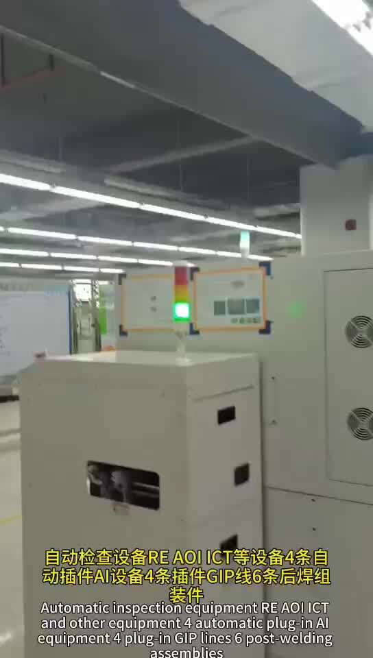
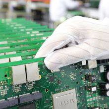
Multi Layer PCBA, SMT, DIP, and Post Soldering Production Process Control


Related Products
-
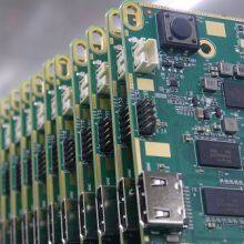
 16 Layer HDIPCB+PCBA (SMT+rear Welding+plug-in)US$ 10 - 12MOQ: 1 Pair
 -
Product Design, PCBA Development, PCBA ProcessingUS$ 3.0 - 4.0MOQ: 1000 Sets
-
FPC+PCBA Design and ProductionUS$ 1.5 - 2MOQ: 1000 Sets
-
10 Layer PCB+PCBAUS$ 2 - 3MOQ: 10 Sets
-
Multi Layer Layered Soft Board FPC, Soft Hard Combination FPCUS$ 1.0 - 1.2MOQ: 10 Sets
The production process of multi-layer PCBA (multi-layer printed circuit board components) involves multiple links such as SMT (surface mount technology), DIP (through-hole insertion technology), and post soldering. Process control needs to cover all elements of "human, machine, material, method, environment, and testing" to ensure stable product quality. The following is an explanation of the processes, key control points, and general control elements in each stage:
1、 Overview of Multi Layer PCBA Production Process
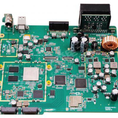
The core of multi-layer PCBA is to complete component assembly on multi-layer PCB boards (usually 4-20 layers, connected by vias between layers), and the overall process is as follows:
PCB incoming inspection → SMT (solder paste printing → mounting → reflow soldering → testing) → DIP (plug-in → wave soldering/immersion soldering → trimming → testing) → post soldering (manual repair soldering/irregular part soldering → trimming) → final inspection → testing
2、 SMT process control (surface mount process)
SMT is used to mount chip and miniaturized components (such as resistors, capacitors, ICs, BGAs, etc.) onto the surface solder pads of PCBs. It is the core component of multi-layer PCBA, with a focus on "high precision, low damage" control.
1. Process steps
PCB pre-treatment: Remove the oxide layer and oil stains on the surface of the PCB (use plasma cleaning if necessary), check the flatness of the solder pads (multi-layer boards are prone to micro deformation due to stress and need to be tested with a laser leveling instrument).
Solder paste printing: Apply solder paste (solder paste) evenly onto PCB pads through a steel mesh.
Component mounting: The surface mount machine uses visual positioning to accurately place components onto solder paste.
Reflow soldering: Melting solder paste through a high-temperature furnace to form solder joints that fix components.
Inspection: Check the quality of solder joints through AOI (Automatic Optical Inspection) or X-Ray (for concealed solder joints such as BGA).
2. Key control points
Standard/parameter examples for key control points in the process
Solder paste printing steel mesh matching: Design steel mesh thickness (0.1-0.2mm) and hole size (1:0.9 ratio to solder pad) based on component type (such as 0201/0402 components, BGA);
Printing parameters: Scraper pressure (5-15N), speed (20-50mm/s), demolding distance (0.5-2mm), to prevent solder paste from having too little/too much tin/bridging. Steel mesh opening tolerance ± 0.01mm; solder paste coverage rate after printing ≥ 95%
Component mounting positioning accuracy: mounting error ≤ ± 0.05mm (for 0201 component), ± 0.1mm (for QFP);
Mounting pressure: 0.1-0.5N (to prevent damage to PCB pads or cracking between layers of multi-layer boards);
Nozzle matching: Select based on component size (e.g. 0.3mm nozzle for 0201, specialized nozzle for BGA). Mounting offset rate ≤ 0.1%
Reflow soldering temperature curve: set according to the type of solder paste (lead-free solder paste melting point 217 ℃+), heating rate ≤ 3 ℃/s, constant temperature zone (150-180 ℃) 60-90s, peak temperature 240-260 ℃ (stay for 5-10 seconds);
Prevent deformation of multi-layer boards: Install support rails inside the furnace with a temperature difference of ≤ 5 ℃ (to avoid interlayer stress). Solder joint wetting rate ≥ 90%; PCB deformation ≤ 0.2%
AOI detection: Identify virtual soldering, bridging, missing parts, and wrong parts;
X-Ray inspection: For BGA and CSP bottom solder joints (multi-layer board solder joints may be obstructed by components), check the solder ball diameter (± 10%) and the absence of voids (void rate ≤ 25%). AOI missed detection rate ≤ 0.01%; X-Ray void exceedance rate ≤ 0.1%
3. Common problems and solutions
Solder paste printing bridging: steel mesh opening too large → reducing opening size; Insufficient scraper pressure → Increase pressure to 10N.
BGA solder joint voids: insufficient reflow peak temperature → increased to 250 ℃; Insufficient volatilization of flux in solder paste → Extend the constant temperature time to 80 seconds.
PCB deformation: When the thickness of the multi-layer board is ≥ 1.6mm, an intermediate support should be added in the furnace to control the deformation within 0.15%.
3、 DIP process control (through-hole insertion process)
DIP is used for assembling components that require passing through PCB through holes (such as connectors, electrolytic capacitors, transformers, etc.), which need to match the accuracy of the through holes on multi-layer boards, with the focus on "correct insertion+reliable solder joints".
1. Process steps
Plugin: Manual or automatic plugin machine inserts component pins into PCB through holes.
Wave soldering/immersion soldering: forming through-hole solder joints by melting solder.
Trimming feet: Trim excess pins (leaving 1-2mm in length).
Inspection: Visual or AOI inspection of solder joints (through-hole filling rate, no virtual soldering).
2. Key control points
Standard/parameter examples for key control points in the process
Plug in error prevention: Use error prevention material racks and plug icon to identify polarity (such as positive and negative poles of electrolytic capacitors);
Pin alignment: Ensure that the pins are inserted vertically (multi-layer board through-hole tolerance ± 0.05mm, skewing can easily cause card holes or PCB delamination). Wrong insertion rate ≤ 0.05%; Pin skew angle ≤ 5 °
Wave soldering flux spraying: uniform atomization amount (100% coverage), preventing excessive residue from corroding multi-layer boards;
Solder parameters: lead-free solder temperature of 260-270 ℃, conveyor speed of 1-1.5m/min, peak height covering 2/3 of PCB thickness. The filling rate of through-hole solder joints is ≥ 75%; No pinholes/bubbles
Precision of the foot cutting knife: The incision is flat (without burrs), leaving a length of 1-2mm (too short leads to insufficient welding strength, too long is prone to short circuit). Burr height ≤ 0.1mm; length deviation ± 0.2mm
3. Common problems and solutions
Plug in card holes: There are burrs in the through holes of multi-layer boards → PCB incoming materials require deburring process; Pin too thick → Replace matching components.
Peak soldering point pulling: soldering temperature too low → increased to 265 ℃; The conveyor belt speed is too fast → reduced to 1.2m/min.
4、 Post welding process control (repair welding and welding of irregular parts)
Post welding is aimed at scenarios that cannot be covered by SMT/DIP, such as large volume connectors, irregular structural components, or defective solder joints before welding repair. It relies on manual operation and the control focus is on "operation specifications+solder joint quality".
1. Process steps
Preprocessing: Clearly identify the repair welding/welding position (mark the defective points), and prepare tools (anti-static soldering iron, hot air gun).
Manual welding: Follow the steps of "heating → tinning → removing tin wire → cooling".
Trimming and Cleaning: Remove bridging and burrs, clean flux residue with isopropanol (to prevent multi-layer board corrosion).
2. Key control points
Standard/parameter examples for key control points in the process
Welding tool soldering iron temperature: ordinary solder joints 320-350 ℃, sensitive components (such as CMOS chips) 280-300 ℃;
Anti static: The grounding resistance of the soldering iron is ≤ 1M Ω, and the operator should wear a grounding wristband (resistance 1-100M Ω). Temperature fluctuation ± 5 ℃; No ESD damage (chip test qualified)
The quality of manual solder joints should be "round and free of virtual soldering": the solder covers ≥ 90% of the solder pads, without bridging (when the distance between adjacent solder joints is ≥ 0.2mm). Virtual soldering rate ≤ 0.1%; Bridge failure ≤ 0.05%
3. Common problems and solutions
Virtual soldering: pad oxidation → lightly grind the pad with fine sandpaper; The temperature of the soldering iron is insufficient → increase to 340 ℃.
ESD damage: Protect sensitive components with anti-static bags before welding → 100% functional testing after welding.
5、 General control elements (applicable throughout the entire process)
ESD protection: Multi layer PCBA contains a large number of ICs and requires full anti-static throughout the process:
Environment: Anti static floor (grounding resistance 10 ^ 6-10 ^ 9 Ω), ion fan (balanced voltage within ± 50V);
Personnel: Wear anti-static clothing/shoes and monitor in real-time with a wristband (alarm resistance100M Ω).
Environmental control:
Temperature and humidity: SMT/DIP workshop 23 ± 3 ℃, humidity 40% -60% (to prevent solder paste from absorbing moisture and PCB deformation);
Cleanliness: Class 10000 (≥ 0.5 μ m particles ≤ 10000 per cubic foot), reducing bridging caused by dust.
Material Management:
Traceability: Print a unique QR code on the PCB, associate component batches, equipment parameters, and operators (recorded using MES system);
Storage: IC low-temperature storage (-10 ° C to 5 ° C), solder paste refrigeration (2-10 ° C), and a 4-hour return to temperature upon retrieval (moisture resistant).
Equipment maintenance:
SMT SMT SMT machine: daily calibration of nozzle positioning (error ≤ 0.01mm), weekly cleaning of lens;
Reflow soldering/wave soldering: Calibrate the temperature sensor weekly (with an error of ± 1 ℃), and clean the solder slag in the furnace every month.
Through the above controls, it can be ensured that the yield of multi-layer PCBA in SMT, DIP, and post soldering processes is ≥ 99%, meeting the requirements of high density and high reliability (such as in the fields of automotive electronics and industrial control)

Send Inquiry to This Supplier


You May Also Like
-
10 Layer PCB+PCBA,High Frequency Circuit Board PCBA,46 Layer PCB+PCBA (SMT)US$ 2 - 3MOQ: 10 Sets
-
8-layer Seam Human-machine Electric Vehicle Motherboard PCBA,SMTUS$ 10 - 12MOQ: 1 Pair
-
18 Layer Power System Motherboard PCBA (SMT+AI+DIP)US$ 10 - 12MOQ: 1 Pair
-
32 Layer High-frequency US Military Product PCBA(SMT+PCBA+DIP)US$ 0.80 - 1.50MOQ: 10 Sets
-
Soft Hard Combination FPCUS$ 2.0 - 3.0MOQ: 10000 Pairs
-
Multi Layer Flexible FPCUS$ 1.2 - 2.0MOQ: 10000 Bags
-
Military System Products,36 Layer BoardUS$ 2.0 - 3.6MOQ: 10000 Bags
-
Multi Layer Flexible FPCUS$ 1000 - 1500MOQ: 50 Ounces
-
Automotive Products, 18 Layers of Any Order HDI Multilayer PCBUS$ 10 - 12MOQ: 0 Short Ton
-
16 Layers, 5 Steps, Multi-layer PCB With 5 StepsUS$ 2 - 3MOQ: 1 Pack


