

Home > Electrical & Electronics > Electrical Control System > SHINKAWA MP-2W2 Machine Protection Monitor
Negotiable
MOQ: 1 Piece (Price negotiable depending on order volume and customization)
Key Specifications
Get Latest Price
Material:
Other, Global universal model
Condition:
Other, Global universal model
Task:
Other, Global universal model
Payment & Shipping
Payment Methods:
Port of Shipment:
China
Delivery Detail:
Delivery time depends on order quantity.
Related Products
-
 SHINKAWA VM-5H3 Machine Protection MonitorNegotiableMOQ: 1 Piece
 -
SHINKAWA VM-5P3 Machine Protection MonitorNegotiableMOQ: 1 Piece
-
SHINKAWA VM-5Z4 Machine Protection MonitorNegotiableMOQ: 1 Piece
-
TEWS TPMC866-11 Industrial Control ModuleNegotiableMOQ: 1 Unit
-
Fireye 85UVF1-1QD Flame MonitorNegotiableMOQ: 1 Unit
Material
Other, Global universal model
Condition
Other, Global universal model
Task
Other, Global universal model
Mathematical Model
Other, Global universal model
Signal
Other, Global universal model
Customized
Non-Customized
Structure
Other, Global universal model
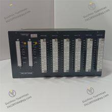
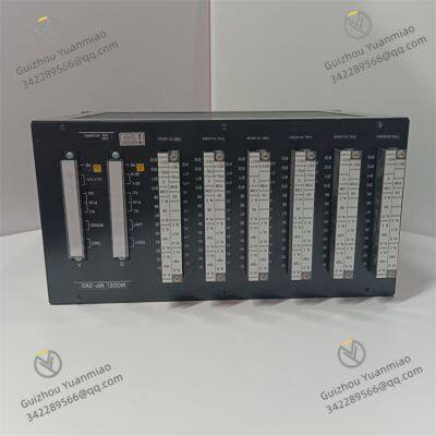
SHINKAWA MP-2W2I. OverviewII. Functional FeaturesIII. Technical Parameters

Send Inquiry to This Supplier

* Email
Want the best price?
Post an RFQ now!

1Yr
Business Type
Trading Company
Year Established
2014
Factory Size
1,000-3,000 square meters
Product Certifications
SA8000
You May Also Like
-
METSO D202275 Programmable Logic Controller (PLC) ModuleNegotiableMOQ: 1 Unit
-
SIGMATEK DNC115 Digital ControllerNegotiableMOQ: 1 Unit
-
AMAT 0100-71267 Control ModuleNegotiableMOQ: 1 Unit
-
PIONEER MAGNETICS PM3398B-6-1-3-E 80026-172-24 Power ModuleNegotiableMOQ: 1 Unit
-
PIONEER MAGNETICS HYRSP-1500-56 Power ModuleNegotiableMOQ: 1 Unit
-
Pacific Scientific SCE904AN-002-01 Axis Servocontroller UnitNegotiableMOQ: 1 Unit
-
Pacific Scientific SCE905AN-002-01 Axis Servocontroller UnitNegotiableMOQ: 1 Unit
-
Pacific Scientific SCE903A3-002-01 Servo DriveNegotiableMOQ: 1 Unit
-
Pacific Scientific PC834-001-T Servo DriveNegotiableMOQ: 1 Unit
-
SHINKAWA MP-2S Dual Vibration MonitorNegotiableMOQ: 1 Unit


