








 Contact Platform Support
 Help Center
A3p400-fgg256i Programmable Logic Device (CPLD / FPGA) MICROSEMI Original Stock



Related Products
-
 Stm8af6226tay st (st) Original StockNegotiableMOQ: 1 Piece
 -
S912zvml12f3wkh 16 Bit Microcontroller - MCU NXP Original StockNegotiableMOQ: 1 Piece
-
Sn6505bdbvr Professional Power Management Ti Original SpotNegotiableMOQ: 1 Piece
-
Ina190a1qdckrq1 Current Sense Amplifier Ti Original StockNegotiableMOQ: 1 Piece
-
Tps62826dmqr Switching Regulator Ti Original StockNegotiableMOQ: 1 Piece
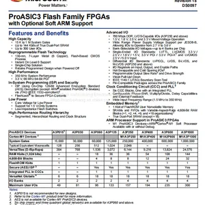
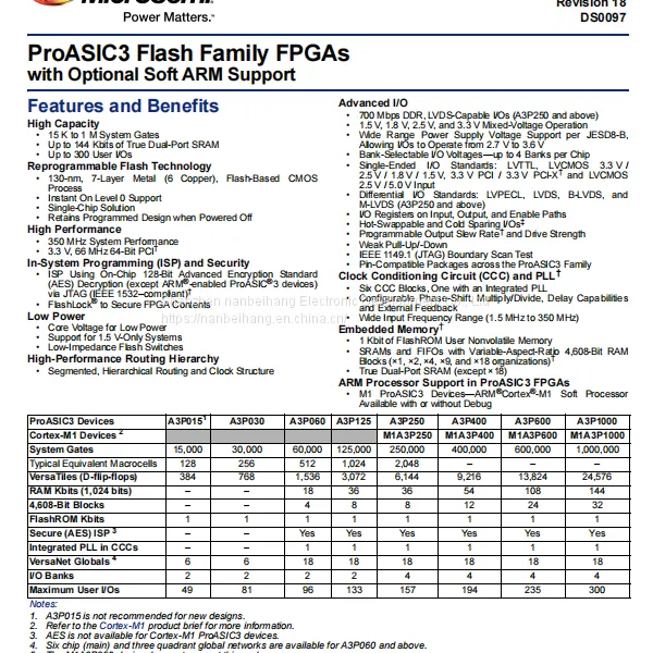
Features and Benefits
High Capacity
• 15 K to 1 M System Gates
• Up to 144 Kbits of True Dual-Port SRAM
• Up to 300 User I/Os
Reprogrammable Flash Technology
• 130-nm, 7-Layer Metal (6 Copper), Flash-Based CMOS
Process
• Instant On Level 0 Support
• Single-Chip Solution
• Retains Programmed Design when Powered Off
High Performance
• 350 MHz System Performance
• 3.3 V, 66 MHz 64-Bit PCI†
In-System Programming (ISP) and Security
• ISP Using On-Chip 128-Bit Advanced Encryption Standard
(AES) Decryption (except ARM®-enabled ProASIC®3 devices)
via JTAG (IEEE 1532–compliant)†
• FlashLock® to Secure FPGA Contents
Low Power
• Core Voltage for Low Power
• Support for 1.5 V-Only Systems
• Low-Impedance Flash Switches
High-Performance Routing Hierarchy
• Segmented, Hierarchical Routing and Clock Structure
Advanced I/O
• 700 Mbps DDR, LVDS-Capable I/Os (A3P250 and above)
• 1.5 V, 1.8 V, 2.5 V, and 3.3 V Mixed-Voltage Operation
• Wide Range Power Supply Voltage Support per JESD8-B,
Allowing I/Os to Operate from 2.7 V to 3.6 V
• Bank-Selectable I/O Voltages—up to 4 Banks per Chip
• Single-Ended I/O Standards: LVTTL, LVCMOS 3.3 V /
2.5 V / 1.8 V / 1.5 V, 3.3 V PCI / 3.3 V PCI-X† and LVCMOS
2.5 V / 5.0 V Input
• Differential I/O Standards: LVPECL, LVDS, B-LVDS, and
M-LVDS (A3P250 and above)
• I/O Registers on Input, Output, and Enable Paths
• Hot-Swappable and Cold Sparing I/Os‡
• Programmable Output Slew Rate† and Drive Strength
• Weak Pull-Up/-Down
• IEEE 1149.1 (JTAG) Boundary Scan Test
• Pin-Compatible Packages across the ProASIC3 Family
Clock Conditioning Circuit (CCC) and PLL†
• Six CCC Blocks, One with an Integrated PLL
• Configurable Phase-Shift, Multiply/Divide, Delay Capabilities
and External Feedback
• Wide Input Frequency Range (1.5 MHz to 350 MHz)
Embedded Memory†
• 1 Kbit of FlashROM User Nonvolatile Memory
• SRAMs and FIFOs with Variable-Aspect-Ratio 4,608-Bit RAM
Blocks (×1, ×2, ×4, ×9, and ×18 organizations)†
• True Dual-Port SRAM (except ×18)
ARM Processor Su

Send Inquiry to This Supplier


You May Also Like
-
Ds90ub949trgcrq1 Serializer / Deserializer Ti Original StockNegotiableMOQ: 1 Piece
-
Bts5010-1ekb Pg-dso-14 Power Switch IC Has the Lowest PriceNegotiableMOQ: 1 Piece
-
Tps3700dser Wson-6 Analog Comparator Price DiscountNegotiableMOQ: 1 Piece
-
Opa348aidckr op Amp Ti Original SpotNegotiableMOQ: 1 Piece
-
Lm25141qrgerq1 Switch Controller Ti Original StockNegotiableMOQ: 1 Piece
-
Tps65283rger Switching Regulator Ti Original StockNegotiableMOQ: 1 Piece
-
Cy8c27543-24axi Embedded Microcontroller Cypress Original StockNegotiableMOQ: 1 Piece
-
Sak-tc1782f-320f180hr BA Pg-lqfp-176 Infineon Original StockNegotiableMOQ: 1 Piece
-
L9301-tr Door Driver st Original StockNegotiableMOQ: 1 Piece
-
S912xeg128j2maar 16 Bit Microcontroller - MCU NXP Original StockNegotiableMOQ: 1 Piece


