

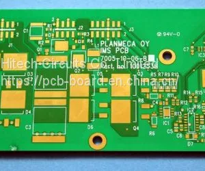
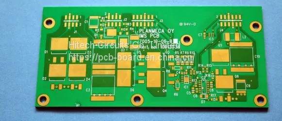
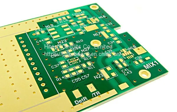
Heavy Copper 6oz 6L High TG Material With 2.80mm Board Thickness and ENIG Surface Treatment Pcb

Related Products
-
 China One-stop PCBA Service And PCB Component Assembly/printer Controller PCB AssemblyUS$ 0.002 - 0.1MOQ: 0 Square Meter
 -
China Customized Fr4 Prototype Pcb AssemblyUS$ 0.002 - 0.1MOQ: 0 Square Meter
-
High TG Black V-cut Pcb Fabrication With Gold FingersUS$ 0.002 - 0.1MOQ: 0 Square Meter
-
Custom Printed Circuit Boards Supplier/Immersion Silver PCBUS$ 0.002 - 0.1MOQ: 0 Square Meter
-
High Quality and Low Cost Prototype PCB Circuit BoardUS$ 0.002 - 0.1MOQ: 0 Square Meter
Heavy copper 6oz 6L High TG material with 2.80mm Board thickness and ENIG surface treatment pcb
Why us?
1.We are PCB & PCB assembly manufacturer with 12 years experience
2.UL&Rohs&ISO9001 certificated
3.4 times 100% QC inspection before Shipping.
4. Profeesional one-stop service release your energy to focus on design and marketing.
5.First order delivery time is around 15days, next order we will produce enough goods in stock for long cooperation.
6.Sign NDA to keep your design safe.
Our Service:
1. We will reply for you within 24hours once we get your inquiry.
2.Design and produce almost any LED pcb as your requirement.
3.We can offer you unique design and some our current models.
4.100%testing guarrantees stable quality, ISO 9001:2000 ,UL, RoHS certification
Lead Time:
| Lead time for sample | 2~3days for single-side board |
| 4~5days for double-side board | |
| 24~48hours for ugent | |
| Lead time for opening mould | 3~5days for normal mould |
| 5~7days for hard mould | |
| Lead time for mass production | 5~7days for single/double board |
Company Information:
Hitech focuses on high-mix, low volume and quick turn pcb service. With a special market position and excellent corporate culture, we can provide "One-stop shop" service from 1 to 26 layers of PCB products, which includs double layers PCB, Multilayer PCB, Aluminium PCB (Metal core PCB) Flexible PCB (FPCB), Rigid-Flex PCB (Flex-rigid PCB), High Density Interconnect (HDI )PCB boards, heavy copper boards, buried Capacitance & resistance boards, etc. Our products cover various products are exported to Europe, America and Asia.
Detailed specification of manufaturing capacity:
| NO | Item | Craft Capacity |
| 1 | Layer | 1-30 Layers |
| 2 | Base Material for PCB | FR4, CEM-1, TACONIC, Aluminium, High Tg Material, High Frequence ROGERS ,TEFLON, ARLON, Halogen-free Material |
| 3 | Rang of finish baords Thickness | 0.21-7.0mm |
| 4 | Max size of finish board | 900MM*900MM |
| 5 | Minimum Linewidth | 3mil (0.075mm) |
| 6 | Minimum Line space | 3mil (0.075mm) |
| 7 | Min space between pad to pad | 3mil (0.075mm) |
| 8 | Minimum hole diameter | 0.10 mm |
| 9 | Min bonding pad diameter | 10mil |
| 10 | Max proportion of drilling hole and board thickness | 1:12.5 |
| 11 | Minimum linewidth of Idents | 4mil |
| 12 | Min Height of Idents | 25mil |
| 13 | Finishing Treatment | HASL (Tin-Lead Free), ENIG(Immersion Gold), Immersion Silver , Gold Plating (Flash Gold), OSP, etc. |
| 14 | Soldermask | Green, White, Red, Yellow, Black, Blue, transparent photosensitive soldermask, Strippable soldermask. |
| 15 | Minimun thickness of soldermask | 10um |
| 16 | Color of silk-screen | White, Black, Yellow ect. |
| 17 | E-Testing | 100% E-Testing (High Voltage Testing); Flying Probe Testing |
| 18 | Other test | ImpedanceTesting,Resistance Testing, Microsection etc., |
| 19 | Date file format | GERBER FILE and DRILLING FILE, PROTEL SERIES, PADS2000 SERIES, Powerpcb SERIES, ODB++ |
| 20 | Special technological requirement | Blind & Buried Vias and High Thickness copper |
| 21 | Thickness of Copper | 0.5-14oz (18-490um) |
Equipment List:
| NO. | Machine Name | QTY | NO. | Machine Name | QTY |
| 1 | PRESS | 2 | 10 | Exposurer | 5 |
| 2 | X-Ray | 1 | 11 | Deveoloper | 3 |
| 3 | Brown-Oxidation | 1 | 12 | Auto V-cut | 1 |
| 4 | Drilling | 13 | 13 | AOI | 2 |
| 5 | Cutter | 1 | 14 | Routing | 7 |
| 6 | PTH | 1 | 15 | ETS | 12 |
| 7 | PAL | 1 | 16 | Fly Probe | 4 |
| 8 | PAT | 1 | 17 | YAMAHA SMT | 3 |
| 9 | Flash Gold | 1 | 18 | FUJI SMT | 4 |
Quotation requirements for PCB and PCB Asssembly project:
- Gerber File and Bom List;
- Quote Quantity;
- Advise your technical requirements for quoting reference;
- Clearly picturers of PCB or PCB Assembly Sample to us for reference;
- Test Mothod for PCB Assembly.
Mobile:+86-17875743770
Wechat:1634005492(QQ)
Tel: +86-755-29630063-804
Email: sales10(at)hitechcircuits(dot)com
Website:

Send Inquiry to This Supplier


You May Also Like
-
Heavy Copper PcbUS$ 0.5 - 2.5MOQ: 1 Piece
-
Heavy Copper PCB Board, High Quality PCB BoardUS$ 0.2 - 1.5MOQ: 1 Piece
-
Extra Large Heavy Copper PCB Board CustomUS$ 0.5 - 1.5MOQ: 1 Piece
-
High Level Heavy Copper Pcb Leading Pcb e Cigarette Pcb Circuit BoardUS$ 0.02 - 2MOQ: 1 Square Meter
-
Heavy Copper 6oz 6L High TG Material With 2.80mm Board Thickness and ENIG Surface Treatment PcbUS$ 0.002 - 0.1MOQ: 0 Square Meter
-
4Layer With Heavy Copper 3OZ Used for Industry Control From ChinaUS$ 0.2 - 0.5MOQ: 1 Piece
-
Copper Clad Ground Rod 25mm 1" x 1500mm 2000mm 2400mm Extra Heavy Industrial EarthingUS$ 8 - 25MOQ: 100 Kilograms
-
Heavy Copper Core PCB Board With Quick Turn PCBUS$ 0.56 - 0.95MOQ: 1 Piece
-
Copper Sheet 0.3mm Copper Plate Sheet 1.6mm 35um Copper PcbUS$ 8 - 10MOQ: 1000 Kilograms
-
Inlaid Thick Copper Bent PCB,Bent Copper Electrolytic PCB,8W Adhesive PCBNegotiableMOQ: 100 Units


