








 Contact Platform Support
 Help Center
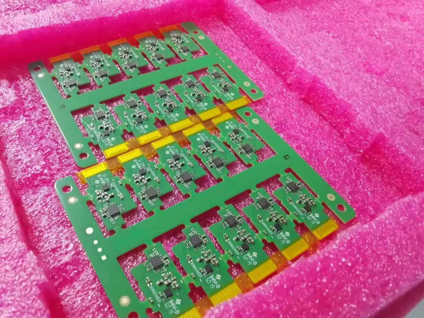
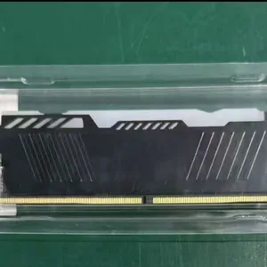
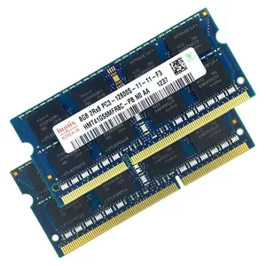
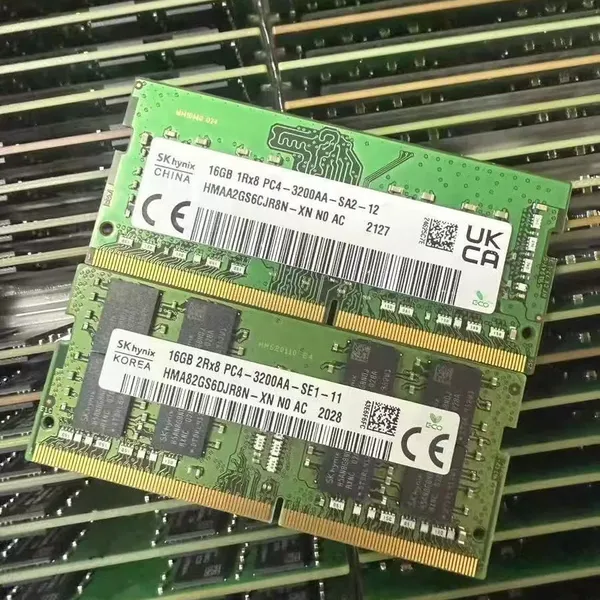
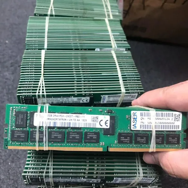
China Chaosheng Electronic Memory Module - Server - Graphics Card - Memory Card, Electronic Thick Gold Finger PCB Process Description
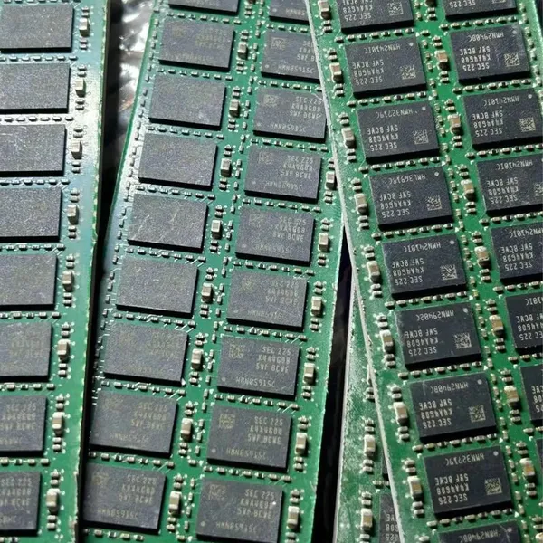
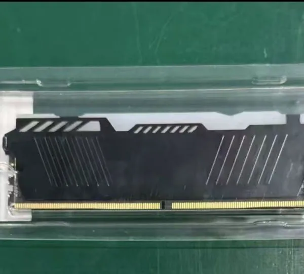
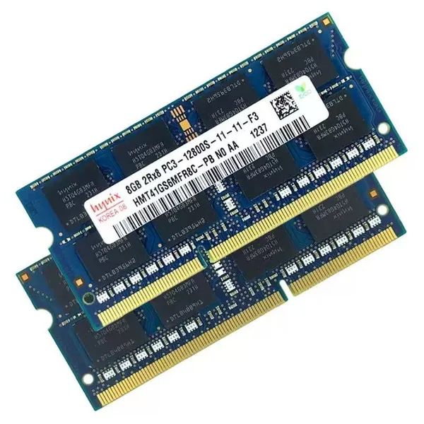
Product Spotlights



Related Products
-
 China Chaosheng Electronics Desktop Computer Memory Module - Server - Graphics Card - Memory Card Electronic Thick Gold Finger PCB Process DescriptionNegotiableMOQ: 1 Blade
 -
12 Layers, 3rd Order Gold Finger Circuit Board PCB,multi-layer Step HDIPCBNegotiableMOQ: 20 Units
-
10 Layers, 2nd Order Gold Finger Circuit Board PCB,18mm Multi-layer Ultra Thick PCBNegotiableMOQ: 20 Units
-
16 Layers, 3rd Order Gold Finger Circuit Board PCB,Graphics Card Gold Finger PCBNegotiableMOQ: 10 Units
-
8 Layers, 3rd Order Gold Finger Circuit Board PCB,Electric Thick Gold Finger PCBNegotiableMOQ: 20 Units
China Chaosheng Electronic Memory Module - Server - Graphics Card - Memory Card, Electronic Thick Gold Finger PCB Process Description
1、 Product List&Corresponding Gold Finger Types
1. Computer memory module (DDR4/DDR5)**
DIMM gold fingers, electroplated hard gold, 45 ° beveled edge chamfer
-Consumer grade: Gold thickness * * 0.76 μ m (30 μ in)**
-Industrial/server memory module: * * 1.27 μ m (50 μ in) * *, nickel substrate 3-6 μ m, compliant with JEDEC, IPC-4556 high reliability Class3 standards
-The standard thickness of the board is 1.6mm, and green oil coverage is prohibited in the gold finger area
2. Industrial server board/expansion card**
PCIe 4.0/5.0、 High speed network card, computing power acceleration card
-Industrial server standard: * * hard gold 0.8-1.3 μ m**
-High vibration/long-term uninterrupted working conditions (computer room, industrial control) * * Thick metal 1.5-2.5 μ m**
-Chamfering at 30 °, insertion and removal life ≥ 5000 times, -40~+85 ℃ temperature cycling test
3. Independent graphics card PCB**
PCI Express Gold Finger
-Ordinary gaming graphics card: hard gold * * 0.5~0.8 μ m**
-Workstation/AI server graphics card: * * 1.0-1.5 μ m thick gold**
-1.6mm substrate, high-speed differential impedance of 100 Ω, gold finger window expansion of 0.05-0.1mm
4. Memory card/Data storage card (SD/MicroSD/CF)**
Edge contact gold fingers, locally thick gold plating
-Consumer SD card: hard gold 0.4-0.6 μ m
-Industrial wide temperature storage card: * * thick gold ≥ 0.8 μ m * *, wear-resistant, moisture-proof, salt spray resistant, suitable for monitoring, vehicle mounted, and industrial control storage devices
> ⚠️** Key differentiation of processes**
>Gold fingers must be electroplated with Hard Gold (cobalt alloy containing gold, high hardness and wear resistance HV ≥ 130);
>Ordinary sinking gold ENIG soft gold * * cannot be used for inserting and removing gold fingers * *, it is prone to abrasion, oxidation, and poor contact
2、 General Technical Indicators for Thick Gold Fingers (Industrial Edition)
Project | Industrial Gold Standards|
Coating structure | Bottom nickel 3-6 μ m+surface hard gold|
Gold plating thickness (gold layer) | Conventional thick gold: * * 0.8-1.3 μ m * *; Ultra thick wear-resistant customization: 1.5~3.0 μ m|
Chamfering | Memory module 45 °; PCIe graphics card/server board 30 ° -45 °, chamfer length 0.4-0.8mm|
Contact resistance | Initial ≤ 50m Ω, ≤ 100m Ω after 5000 insertions and removals|
Execution standard | IPC-4556, IPC-6012 Class2-Class3 high reliability level|
Testing | X-RF coating thickness measurement, AOI appearance, conductivity, wear resistance testing|
3、 Electric Thick Gold Finger Circuit Board PCB Classification
Thick Gold Finger Circuit Board, Memory Module PCB, DDR5 Memory Board, Server Gold Finger Board, Graphics Card PCB, PCIe High Speed Board, SD Memory Card Contact Board, Partially Plated Hard Gold PCB, Industrial Grade High Wear Resistant Gold Finger, Thick Gold Plated Edge Connector Circuit Board
English Keywords
Thick hard gold finger PCB, DDR5 memory module PCB, server DIMM board, graphic card PCB, PCI‑Express edge connector board, SD memory card contact board, selective electroplated hard gold, industrial high‑wear gold finger circuit board
Complete production process of thick gold finger (electroplated hard gold) circuit board
>Applicable: Memory modules, DDR5 memory boards, server PCIe cards, graphics cards, SD memory card contact boards; **Process=Selective electroplating of hard gold, not immersion gold ENIG**
Overall Process Overview
Inner layer lamination → drilling → copper plating+electroplating → outer layer wiring → graphic electroplating → etching → * * gold finger selective electroplating (thick nickel+thick hard gold) * * → solder mask green oil → silk screen printing → CNC molding → * * gold finger beveled edge chamfering * * → electrical testing → surface post-treatment → final inspection packaging
Step by step explanation (with a focus on highlighting the special processes exclusive to gold fingers)
1. Front end basic PCB production (ordinary multi-layer board process)
1. Inner layer cutting, dry film, etching AOI、 Browning
2. Multi layer lamination
3. CNC drilling, deburring, and adhesive residue removal
4. Chemical deposition of copper+full plate electroplating of copper to ensure hole conductivity and compliance with basic copper thickness standards
5. Expose and develop the outer dry film to create an outer circuit pattern
6. Graphic electroplating of copper and tin protection circuits
7. Film stripping, alkaline etching, and tin stripping to obtain a complete outer copper circuit
>**The design must reserve plating Tie Bar * * to connect all gold finger contacts to the edge of the board, which is conductive during gold plating and cut off during molding
2. Gold finger selective electroplating [the core of the entire process]
1. * * Pre treatment * *: degreasing → micro corrosion → acid washing activation, ensuring that the gold finger copper surface is free of oxidation and oil stains, so that the coating will not peel off
2. Masking protection**
Use * * peelable blue adhesive/electroplated high-temperature resistant tape * * to cover the entire board surface, * * only exposing the copper area of the gold finger contacts * *, and prohibiting gold plating on other pads and circuits to save gold salt costs
3. * * Electroplating bottom layer nickel (barrier layer)**
Nickel aminosulfonate electroplating, nickel thickness * * 3.0-6.0 μ m**
Function: Block copper gold interdiffusion, enhance gold layer adhesion, anti-wear substrate
4. * * Electroplating thick hard gold (gold cobalt alloy)**
Adding cobalt element to the gold plating solution to form hard gold with a hardness of HV130-250
-Memory module/server: * * 0.76-1.27 μ m (30-50 μ in)**
-High reliability industrial board, AI graphics card: * * 1.5-2.5 μ m ultra thick gold customization**
-SD Industrial Memory Card Contact: ≥ 0.8 μ m
It is necessary to perform X-RF fluorescence thickness measurement to randomly check the thickness of the gold and nickel layers, in order to prevent the thickness from not meeting the standard
5. Remove glue and wash with water
Tear off the blue adhesive/electroplating tape, wash with multiple layers of water, remove residual chemicals, and avoid corrosion of the board surface
> ⚠️ Key point: Gold finger electroplating must be placed before solder mask. If green oil is applied before gold plating, it is prone to overflow and poor plating
3. Solder mask (green oil)+silk screen printing
1. Whole board printing photosensitive solder mask ink
2. The golden finger area must be windowed, and the green oil must not be pressed against the edge of the golden finger. The window should be widened by 0.05-0.1mm to prevent the green oil from covering the golden finger
3. Exposure and development, solder mask curing
4. Screen printed characters LOGO、 Model and characters are prohibited from being printed in the gold finger area
4. CNC shape milling edge
Milling out the overall outline of the board, * * retaining the gold finger electroplating lead * *, but not completely cutting to the edge of the gold finger yet
5. Golden Finger Diagonal/Chamfering [Exclusive Process]
Use a dedicated beveled edge machine for processing
-DDR memory module: standard * * 45 ° chamfer**
-PCIe graphics card, server board: 30 ° -45 ° optional
-Chamfering depth: 0.4-0.8mm (regular thickness of 1.6mm)
Function: Convenient for inserting cards, eliminating burrs on the board edge, and preventing sharp edges from scratching the slot metal spring
> ⚠️ Chamfering is done after gold plating, with no gold on the chamfered surface. High end products can be re coated with edge gold (at a higher cost)
6. Electrical testing&visual inspection
1. Flying needle/needle bed electrical testing: open short circuit, impedance (high-speed board), focus on checking the conductivity of the gold finger contacts
2. AOI+manual visual inspection: Check for scratches, nickel exposure, blackening, blistering on the coating, and pinholes on the gold fingers
3. X-RF sampling of gold thickness to ensure compliance with the requirements for thick gold
7. Post processing, cleaning, packaging
1. Chemical oxidation prevention treatment, pure water cleaning, and hot air drying
2. Cut off the gold plated leads on the edge of the board
3. Vacuum anti-static bag+desiccant packaging to prevent moisture and oxidation of gold fingers
Comparison of Three Golden Finger Crafts (Selection Reference)
|Craftsmanship | Can achieve gold thickness | Wear resistant insertion and removal | Suitable products|
|Selective electroplating of hard gold (this process) | 0.5-3 μ m thick gold | ★★★★ Over 5000 times | Memory modules, servers, graphics cards, industrial SD cards|
|Chemical immersion gold ENIG | 0.05-0.15 μ m | ★☆ Extremely easy to wear through | Ordinary solder pads, * * strictly prohibited for inserting and removing gold fingers**|
|Full board electroplated gold | Thick gold can be made | Extremely high cost, rarely used|
Factory production must control key parameters (which can be directly sent to PCB suppliers)
1. Coating structure: * * Ni 3-6 μ m+Hard Au (gold cobalt alloy)**
2. Gold layer thickness: Memory module ≥ 1.27 μ m; Consumer graphics card ≥ 0.8 μ m; Server industrial board ≥ 1.5 μ m
3. Chamfering angle and depth tolerance ± 0.05mm
4. Open the window with golden fingers, and do not press the edges with green oil
5. XRF coating thickness detection for each PNL board

Send Inquiry to This Supplier



You May Also Like
-
8 Layers, 3rd Order Gold Finger Circuit Board PCBNegotiableMOQ: 10 Units
-
14 Layers of Gold Finger Circuit Board PCB,Electric Thick Gold Finger PCBNegotiableMOQ: 10 Units
-
16 Layers Golden Finger PCB,Computer Graphics Card Gold Finger PCBNegotiableMOQ: 10 Units
-
Computer Board/graphics Card/memory Module PCB Circuit Board and Gold Finger Thickened Electroplating Core TechnologyNegotiableMOQ: 1 Blade
-
Chaosheng Computer Board/graphics Card/memory Module PCB Circuit Board and Gold Finger Thickened Electroplating Core TechnologyNegotiableMOQ: 1 Blade
-
China Super Sheng Network Card Gold Finger, Computer Board/Graphics Card/Memory Module PCB Circuit Board and Gold Finger Thickened ElectroplatingNegotiableMOQ: 1 Blade
-
Vacuum Packaging+cardboard Packaging China Chaosheng Wireless Network Card Gold Finger PCB, Computer Board PCB/graphics Card/memory Module PCBNegotiableMOQ: 1 Blade
-
China Chaosheng Electronics' Wireless Network Card Gold Finger PCB, Computer Board PCB/graphics Card/memory Module PCB Circuit Board and Gold FingerNegotiableMOQ: 1 Blade
-
Chaosheng Electronic Server Graphics Card Electronic Gold Circuit Board Source FactoryPCBNegotiableMOQ: 1 Blade
-
Chaosheng Electronics Industrial Computer Memory Module Electronic Thick Gold Finger Circuit Board Source FactoryPCBNegotiableMOQ: 1 Blade


