

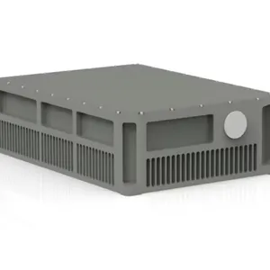
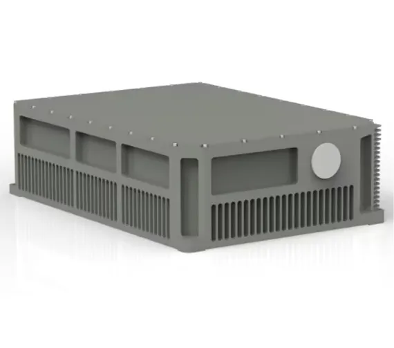
1342nm Solid-state Laser
Product Spotlights
Related Products
-
 1.5μm/2μm Laser Welding: The \"Light\" Solution for Precision Welding of Transparent PlasticsNegotiableMOQ: 1 Set
 -
1342nm Solid-state LaserNegotiableMOQ: 1 Set
-
1.5μm/2μm Laser Welding: The "Light" Solution for Precision Welding of Transparent PlasticsNegotiableMOQ: 1 Set
-
1.5μm/2μm Laser Welding: The "Light" Solution for Precision Welding of Transparent PlasticsNegotiableMOQ: 1 Set
-
1.5μm/2μm Laser Welding: The "Light" Solution for Precision Welding of Transparent PlasticsNegotiableMOQ: 1 Set
Why 1342nm? The Core Value of the Unique Wavelength
Silicon-based materials exhibit precise absorption characteristics to 1342nm laser light, enabling efficient material removal while minimizing the heat-affected zone and avoiding damage to surrounding precision structures. This property makes it stand out in micron-level precision processing, earning it the industry-recognized title of "golden wavelength".
Compared with traditional light sources, the 1342nm solid-state laser achieves smoother cutting edges and more uniform etching depth in silicon-based processing, providing reliable process guarantees for the manufacturing of high-end semiconductor devices.
Four Core Advantages to Strengthen Product Competitiveness
The product features of this laser perfectly meet the demand for long-term stable operation in industrial environments:
- High reliability and long lifespan: Adopting mature solid-state laser technology, core components have a long service life and can adapt to high-intensity production environments, significantly reducing equipment replacement frequency.
- Excellent beam quality and mature technology: With a beam quality M²
- Capable of long-term continuous operation: Supports 7×24-hour continuous working mode, meeting the capacity requirements of large-scale production in semiconductor factories.
- Simple maintenance and low operating costs: Modular design facilitates daily maintenance, with low consumable consumption, making long-term use costs significantly lower than similar devices.
Diverse Application Scenarios Covering Industrial and Scientific Research Fields
🔹 Industrial Manufacturing
1. Silicon Wafer Stealth Dicing: Uses 1342nm laser to form a modified layer inside the silicon wafer, achieving stress-free and debris-free wafer separation, especially suitable for processing ultra-thin and large-size wafers.
2. Integrated Circuit (IC) Trimming: Performs fine-tuning on precision components such as chip resistors and capacitors to correct circuit parameters and improve chip yield and performance consistency.
3. MEMS Device Manufacturing: Achieves sub-micron precision processing in the structural etching and electrode formation of micro-electro-mechanical systems (such as accelerometers and gyroscopes).
4. Display Panel Repair: Precisely repairs pixel defects and line breaks in OLED and LCD panels to extend their service life.
🔹 Scientific Research and Medical Care
1. Biological Imaging and Diagnosis: Serves as a light source with high penetration depth and high resolution in biological imaging technologies such as optical coherence tomography (OCT).
2. Basic Optical Research: Acts as an ideal light source for spectral analysis and nonlinear optical experiments, supporting cutting-edge scientific exploration.
3. Polymer Micromachining: Enables thermal damage-free precision etching in the manufacturing of polymer microfluidic chips and microlenses.

Send Inquiry to This Supplier


You May Also Like
-
1.5μm/2μm Laser Welding: The "Light" Solution for Precision Welding of Transparent PlasticsNegotiableMOQ: 1 Set
-
1342nm Solid-state LaserNegotiableMOQ: 1 Set
-
1342nm Solid-state LaserNegotiableMOQ: 1 Set
-
High Power Lightweight and Miniaturized 2-micron Laser ModulesNegotiableMOQ: 1 Unit
-
Semiconductor-Pumped Erbium Lasers: A New Benchmark for Efficient and Precise Mid-Infrared Light SourcesNegotiableMOQ: 10 Sets
-
Semiconductor-Pumped Erbium Lasers: A New Benchmark for Efficient and Precise Mid-Infrared Light SourcesNegotiableMOQ: 1 Set
-
2μm Continuous / Quasi-Continuous Fiber Lasers: The "Precision Energy Core" for Cross-Field Applications ✨NegotiableMOQ: 1 Set
-
2μm Continuous / Quasi-Continuous Fiber Lasers: The "Precision Energy Core" for Cross-Field Applications ✨NegotiableMOQ: 1 Set
-
2μm Continuous / Quasi-Continuous Fiber Lasers: The "Precision Energy Core" for Cross-Field Applications ✨NegotiableMOQ: 1 Set
-
2μm Continuous / Quasi-Continuous Fiber Lasers: The "Precision Energy Core" for Cross-Field Applications ✨NegotiableMOQ: 1 Set


