








 Contact Platform Support
 Help Center
Analysis of China Chaosheng's Ultra-Large-Size Large Gold Surface Circuit Board Production Technology
Product Spotlights



Related Products
-
 Oversized Large Copper Surface Thick Gold 20U PCB,Large Sized Drone Circuit Board PCBNegotiableMOQ: 1 Blade
 -
Vacuum Packaging+wooden CratePCB,Ultra Large and Ultra-thin PCBNegotiableMOQ: 1 Blade
-
Hole Board Circuit Board PCB ,Dense Aperture 2.40 Hole Ultra Large Size PCB,Oversized Glass Screen PCBNegotiableMOQ: 1 Blade
-
China Super Sheng, Ultra Large Size Multi-layer Whole Board Gold-plated Circuit Board PCB, Nuclear Product PCBNegotiableMOQ: 1 Blade
-
China Chaosheng Electronics | 1650 × 700mm Ultra Large Size Four Layer 3OZ Thick Copper Nickel Gold Circuit Board PCBNegotiableMOQ: 1 Blade
If you have any needs, please contact us:
whatsapp:+8613528819118
Skype live: pcb-fpcb88@163.com
E-mail : sales@chaoshengpcb-fpc.com
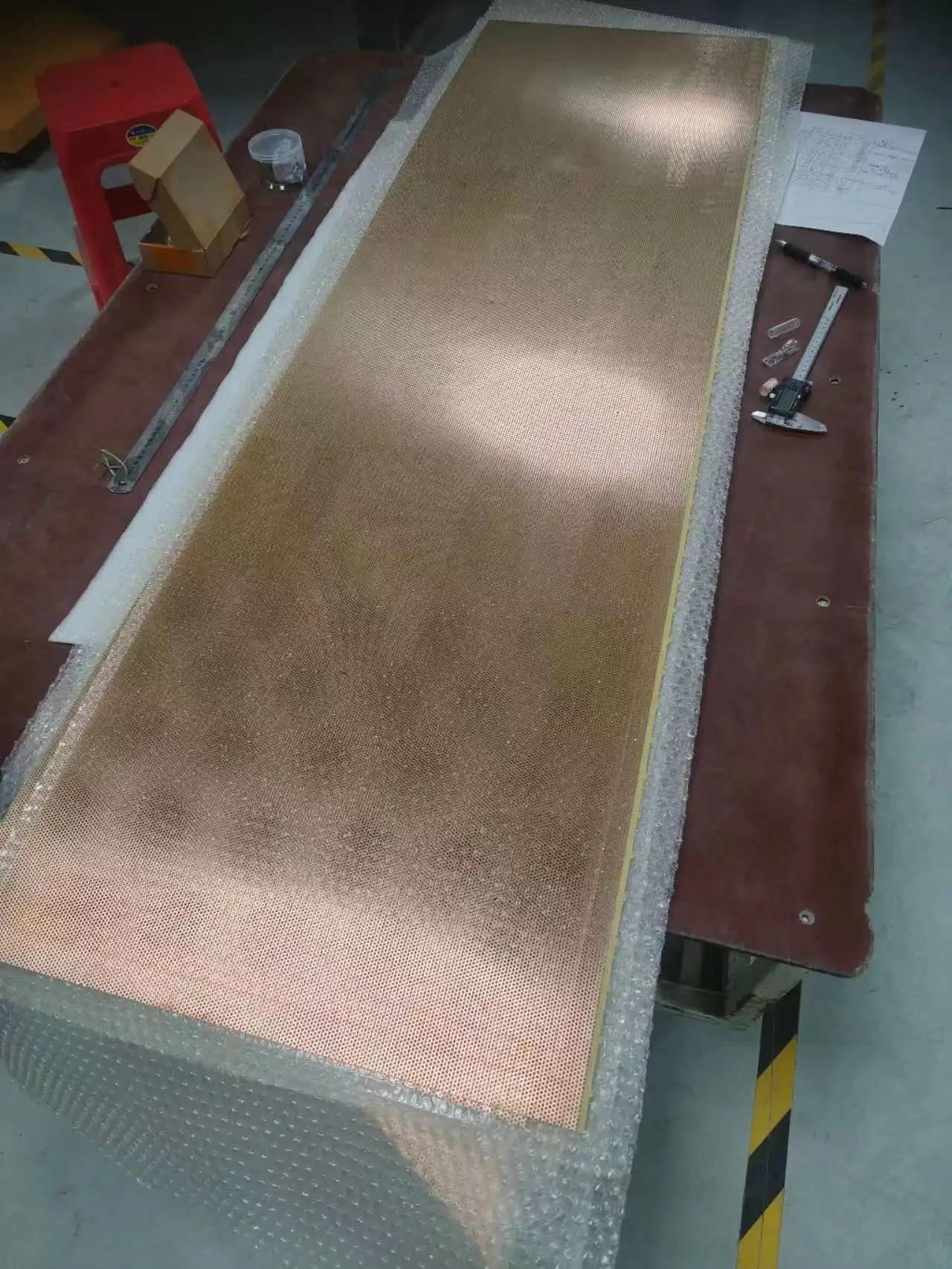
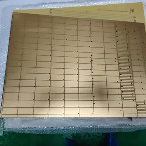
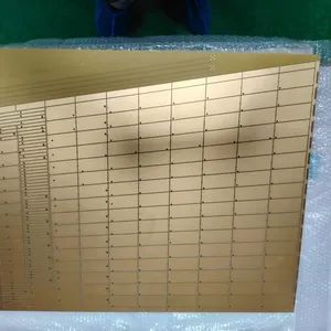
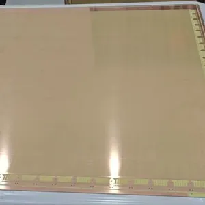
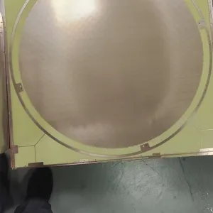
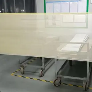
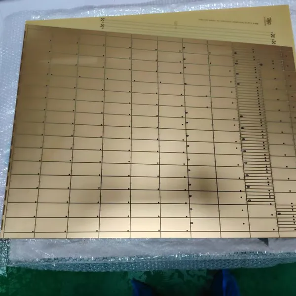
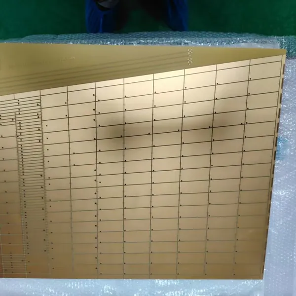
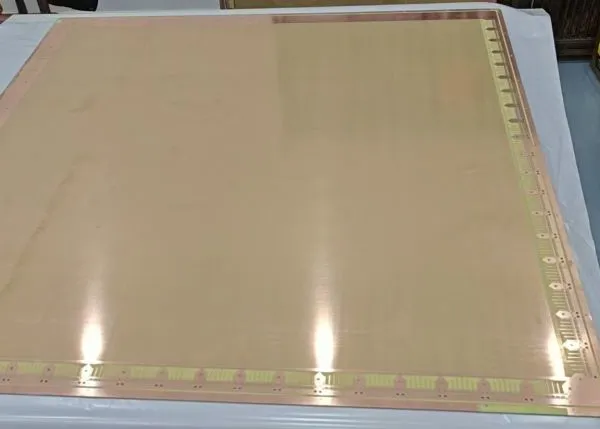
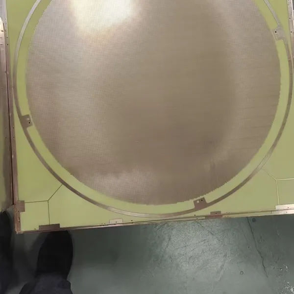
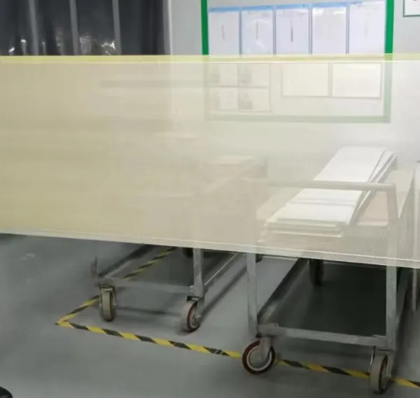
Contact: Mank. Li Analysis of China Chaosheng's Ultra-Large-Size Large Gold Surface Circuit Board Production Technology In the global wave of upgrading the electronics industry toward high performance, integration, and large-scale development, circuit boards serve as the core "backbone" and "neural hub" of electronic devices. Their size specifications and process precision directly determine the performance upper limit of terminal products. Rooted deeply in the electronic manufacturing field, China Chaosheng Group has overcome multiple technical barriers in large gold surface processes and ultra-large-size production by virtue of its profound accumulation in custom ultra-large-size circuit board manufacturing, forming a highly competitive technological system for producing ultra-large-size large gold surface circuit boards. This technology not only fills the domestic technical gap in related fields but also becomes a key core technology supporting the development of strategic emerging industries such as 5G communications, new energy vehicles, industrial automation, and high-end medical care. 1. Overview of Core Technology Chaosheng's ultra-large-size large gold surface circuit board production technology refers to a high-end circuit board manufacturing technology that breaks through conventional size limits to achieve processing of ultra-large panels up to 2600mm × 1300mm. Meanwhile, it adopts large gold surface processes such as immersion gold and electro-nickel gold to form a uniform and dense gold layer coating on the circuit board surface, integrating the advantages of ultra-large-size integration with the excellent electrical conductivity, corrosion resistance, and heat resistance of the gold layer. Its core essence lies in resolving the inherent contradiction between "large size" and "high precision" and "high reliability", realizing gold layer uniformity control, circuit precision guarantee, and structural stability improvement under ultra-large panel conditions. The products cover various structural types including single-layer, double-layer, and 4-80 layer multi-layer boards, with board thickness customizable flexibly between 0.12mm and 10.0mm to meet the personalized needs of different high-end fields. 2. Core Process System Chaosheng's ultra-large-size large gold surface circuit board production technology integrates five core process modules: ultra-large-size substrate processing, high-precision circuit fabrication, large gold surface electroplating, multi-layer lamination, and intelligent inspection. All links work collaboratively to ensure product quality. 2.1 Ultra-Large-Size Substrate Preprocessing Technology The substrate is the foundation for ensuring the stability of ultra-large-size circuit boards. Chaosheng adopts high Tg (glass transition temperature) laminates as the core substrate, reducing the risk of stress deformation during processing from the source. To address the problem that ultra-large-size substrates are prone to warping and damage during cutting and handling, an innovative customized substrate cutting scheme is adopted, combined with special clamping devices to achieve stable transfer of substrates. Meanwhile, plasma cleaning technology is used to remove oil stains, impurities, and oxide layers on the substrate surface, enhancing the adhesion between the substrate and subsequent plating layers and circuits, and laying a stable foundation for subsequent processes. 2.2 High-Precision Circuit Fabrication Technology For ultra-large panels, circuit precision control is the key technical point. Chaosheng has introduced fully automated laser drilling equipment, achieving a drilling precision of ±5μm with a minimum aperture of 0.10mm, which effectively solves the positioning deviation problem during drilling of ultra-large panels. In the pattern transfer process, an ultra-large-size exposure machine with a specification of 2600mm × 1250mm is adopted, combined with Laser Direct Imaging (LDI) technology, realizing an exposure uniformity of ≥93% and a high-precision line width/spacing control of ≤25μm, ensuring the consistency of fine circuits on ultra-large panels. In the etching process, vacuum etching technology is employed, combined with a zonal process control strategy to dynamically adjust the etching rate of different areas, avoiding the problem of over-etching at the edges or under-etching in the center caused by ultra-large panel size, ensuring smooth and burr-free circuit edges, and further improving circuit transmission performance. 2.3 Core Large Gold Surface Electroplating Technology The large gold surface process is a hallmark link of this technology. Chaosheng is equipped with a dedicated immersion gold production line (1650×1200mm) and an electro-nickel gold production line (1400×1200mm). Aiming at the challenge of gold layer uniformity on ultra-large-size panels, the innovative "stepwise electroplating + zonal current regulation" technology is adopted. During the electroplating process, by precisely controlling the temperature, pH value, and current density of the electroplating solution, combined with current distribution simulation of different areas on the panel, the power supply parameters of each area are dynamically adjusted to ensure that the gold layer thickness uniformity deviation is controlled within ±10%. Meanwhile, the pre-treatment activation process is strictly controlled to ensure the adhesion between the gold layer and the underlying copper layer, avoiding defects such as gold layer peeling and blistering. The final gold layer has both excellent electrical conductivity and environmental corrosion resistance, meeting the long-term stable operation requirements of high-end electronic equipment. 2.4 Ultra-Large-Size Multi-Layer Lamination Technology For 4-80 layer ultra-large-size multi-layer large gold surface circuit boards, the lamination process is the core to ensure interlayer bonding strength and dimensional stability. Chaosheng adopts special lamination equipment with an effective lamination size of 2180×1200mm, and innovatively uses a stepwise heating curve and layered pressure application strategy. By accurately calculating the difference in thermal expansion coefficients of substrates between different layers, the temperature and pressure are gradually increased during the lamination process to minimize interlayer stress, effectively controlling the warpage of ultra-large-size multi-layer boards to ≤0.75%, which is far superior to the industry average of 1.5%. Meanwhile, each layer of circuit boards is precisely positioned before lamination, and optical alignment technology is used to ensure interlayer positioning accuracy, avoiding circuit short circuits or open circuits caused by interlayer offset. 2.5 Full-Process Intelligent Inspection Technology To ensure the quality of ultra-large-size large gold surface circuit boards, Chaosheng has built a full-process intelligent inspection system. It adopts AOI (Automatic Optical Inspection) equipment with a total width of 2600×1200mm and laser inspection equipment with a size of 2100×1150mm. High-resolution cameras are used to capture full-panel images, and artificial intelligence image processing algorithms are applied to compare with standard images, which can automatically identify various defects such as hole position deviation, inconsistent external dimensions, missing components, wrong components, solder bridging, and cold soldering, with a defect detection rate of over 99.5%, greatly reducing the product scrap rate. In the finished product testing stage, a special testing machine with a specification of 2600×1200mm is used to achieve comprehensive testing of the electrical performance of ultra-large-size circuit boards, ensuring that products meet the stringent standards of high-end applications. 3. Distinctive Technical Advantages 3.1 Significant Ultra-Large-Size Integration Advantages Relying on a cluster of dedicated ultra-large-size production equipment, Chaosheng can achieve full-specification ultra-large-size processing ranging from 1200×800mm to 2600×1300mm. Among them, double-layer boards can be processed up to 2350×1200mm, and multi-layer buried hole boards up to 1550×1150mm. The ultra-large-size design enables integrated layout of multi-module circuits. For example, in new energy vehicle battery management systems, a circuit board the size of an entire windshield can reduce more than 200 solder joints, which not only greatly improves system reliability but also significantly optimizes heat dissipation performance. 3.2 Fully Automated Production Ensures Stable Quality A fully automated production line from substrate processing to finished product packaging has been established, adopting robot collaborative operations and AGV material transportation to avoid errors and pollution risks caused by manual operations. Key equipment all adopts customized ultra-large-size specifications. For example, fully automatic screen printers and reflow soldering ovens are all matched to the processing needs of 2600mm-level ultra-large panels, achieving seamless connection of various processes and ensuring quality consistency during mass production. 3.3 Strong Process Compatibility and Customization Capability The technology system is compatible with two core types: rigid PCB and flexible FPC. Among them, flexible circuit boards can achieve roll-to-roll continuous processing of 100m × 500mm, which can be bent freely in scenarios such as folding devices and industrial robot joints, integrating both ultra-large-size and flexible characteristics. Meanwhile, special processes such as metal substrate heat dissipation, high-frequency signal transmission, and elastic stretching can be flexibly integrated according to customer needs, meeting the special performance requirements of high-end fields such as medical CT machines and satellite communication equipment. 4. Core Application Fields With its excellent performance, Chaosheng's ultra-large-size large gold surface circuit boards have been widely applied in multiple strategic emerging industries, becoming a core support for promoting the upgrading of related industries. In the new energy vehicle field, they are used in core components such as Battery Management Systems (BMS) and on-board control systems. Ultra-large-size integration reduces solder joints, improving system reliability and heat dissipation efficiency. In the 5G communication and satellite communication field, the large gold surface process ensures low-loss transmission of high-frequency signals, while the ultra-large size meets the integrated design needs of base station equipment and satellite payloads. In the industrial automation field, they are applied to the control backplanes of entire production lines in smart factories, realizing centralized control and collaborative operation of multiple devices. In the high-end medical field, they provide high-precision and high-reliability circuit support for equipment such as CT scanners and nuclear magnetic resonance (NMR) machines. The corrosion resistance of the gold layer ensures the long-term stable operation of equipment in complex medical environments. In addition, this technology is also widely used in high-end consumer electronic models, aerospace, and other fields, boasting broad market application prospects. 5. Development Prospects and Outlook Currently, the global electronics industry is accelerating its evolution toward 5.5G, 6G, intelligent connected vehicles, Industry 4.0, etc., and the demand for ultra-large-size, high-precision, and high-reliability circuit boards will continue to rise. As a leading domestic high-end manufacturing technology, Chaosheng's ultra-large-size large gold surface circuit board production technology will undergo iterative upgrading in three directions in the future: first, further break through size boundaries to develop larger-specification circuit board products to meet the needs of ultra-large integrated equipment; second, optimize the large gold surface process, improve gold layer utilization rate, promote the application of green and environmentally friendly electroplating technologies, and reduce production costs; third, deepen intelligent upgrading, introduce digital twin technology to achieve precise simulation and closed-loop control of the entire production process, and further improve product quality and production efficiency. Driven by policy support, market demand, and technological innovation, Chaosheng's ultra-large-size large gold surface circuit board production technology will continue to lead the development of the domestic high-end circuit board manufacturing industry, helping China's electronic manufacturing industry transform from "scale advantage" to "technological advantage", and providing Chinese solutions and Chinese support for global high-end electronic equipment manufacturing.

Send Inquiry to This Supplier



You May Also Like
-
China Chaosheng Electronics | Aerospace Grade Ultra Large Size 3OZ Thick Copper Four Layer Nickel Gold Printed Circuit BoardNegotiableMOQ: 1 Blade
-
16 Layer Ultra Large Size PCB,double-layer Ultra Large PCB,NegotiableMOQ: 5 Units
-
South Grid System Ultra Large Size Double-layer PCB,Apple Phone Ultra-thin Charging Head PCBNegotiableMOQ: 5 Units
-
2-layer Thick Copper Ultra Large Size Circuit Board PCB,Oversized and Large Hole PCBNegotiableMOQ: 5 Units
-
6 Extra Long Perforated PanelsPCB,Hole Board Circuit Board PCBNegotiableMOQ: 10 Units
-
2-layer Ultra Long Circuit Board PCB,Ultra Long Gong Hollow Board PCB,Multi Layer Ultra Long PCBNegotiableMOQ: 10 Units
-
4 Layers of Ultra Large Thin Circuit Board PCB,Large Sized Drone Circuit Board PCBNegotiableMOQ: 5 Units
-
16L High Frequency Mixed Pressure HDIPCB,Oversized PCBNegotiableMOQ: 10 Units
-
16 Layers, Second Order Ultra Large Size Circuit Board PCB,Multi Layer Ultra,large Size Circuit Board PCBNegotiableMOQ: 1 Unit
-
1 Layer Circuit Board PCB,Oversized and Large Hole PCBNegotiableMOQ: 1 Blade


