

LP3102 Dual Channel Charge Pump Power Solution For TFT LCD Panel Lowpower Semi


Related Products
-
 ME6209A33PG SOT-89-3 MicrOne Low Power Consumption LDO ME6209 SeriesUS$ 0.05 - 0.3MOQ: 10 Pieces
 -
REF195GSZ-REEL7 Analog Devices Voltage References MCROPOWER 5V REF ICUS$ 2.7 - 5MOQ: 1 Piece
-
TL431LIBEDBZRQ1 Texas Instruments Voltage References Automotive, Adjustable, Precision Shunt Regulator With Optimized Reference Current 3-SOT-23 -40 to 150US$ 0.36 - 1MOQ: 1 Piece
-
TP4055 500mA Linear Lithium-ion Battery Charger Top PowerUS$ 0.05 - 0.4MOQ: 10 Pieces
-
PMIC Energy Metering CS5464-ISZ Electronic Component IC Chip Integrated CircuitNegotiableMOQ: 50 Pieces
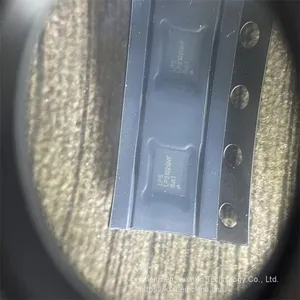
LP3102
Dual Channel Charge Pump Power Solution For TFT LCD Panel
General Description
The LP3102 DC/DC converter integrates two low
noise, high efficiency charge pumps for dual outputs,
which consist of one inverting output and a step-up
output. The device operates from 2.5V to 4.8V input,
and provides a step-up output voltage (VP) of 2x the
input voltage. The negative inverting output (VN) is -1x
inverted from the positive output VP.
The LP3102 is available in a small TDFN-10 pin
package that features a bottom side exposed thermal
pad to provide optimal heat dissipation. The small
package size and low external parts count make the
device ideally suitable for TFT LCD applications of
mobile products. The device is rated to operate from
-40℃ to +85℃ ambient temperature range.
Features
Ultra-Low-Noise for RF Application
2.5V to 4.8V Input Supply Voltage Range
Adaptive 1.5x / 2x mode switchover for positive
voltage and -1x mode for negative voltage
VP output range (VOUT ≦ 2x VIN):
5.5V to 5.9V (LP3102QVF)
VN output range (VOUT ≦ 2x VIN):
-5.5V to -5.9V (LP3102QVF)
High current output: Vin=3.3V, IOUT=±120mA;
Built in Power On Sequence
TDFN-10 (3.0mm × 3.0mm) Package
Absolute Maximum Ratings
Input / Output Voltage to GND --------------------------------------------------------------------------------- -0.3V to 6V
EN to GND -------------------------------------------------------------------------------------------------------- -0.3V to VIN
Maximum Junction Temperature ------------------------------------------------------------------------------------ 150℃
Maximum Soldering Temperature (at leads, 10sec) ----------------------------------------------------------- 260℃
Storage Temperature Range ---------------------------------------------------------------------------- −65℃ to 165℃
Operation Ambient Temperature Range --------------------------------------------------------------- -40℃ to 85℃
Maximum Power Dissipation (PD, TA
Thermal Resistance (JA) --------------------------------------------------------------------------------------------- 68℃/W

Send Inquiry to This Supplier


You May Also Like
-
STR-A6059H Sanken Power IC for PWM Type Switching Power Supply With Low Noise and Low Standby PowerUS$ 0.3 - 4MOQ: 10 Pieces
-
AP64500SP-13 Diodes Incorporated Switching Voltage Regulators DCDC Conv HV Buck SO-8EP(STD) T&R 4KUS$ 0.3 - 2MOQ: 1 Piece
-
BQ76200PWR Texas Instruments Battery Management Fast High Side NCH DriveUS$ 0.3 - 2.7MOQ: 1 Piece
-
MAX809RTRG Onsemi Supervisory Circuits 2.63V uP ResetUS$ 0.07 - 0.35MOQ: 10 Pieces
-
L7905CV STMicroelectronics Linear Voltage Regulators 5.0V 1.5A NegativeUS$ 0.15 - 0.66MOQ: 10 Pieces
-
INA209AIPWR Texas Instruments Current & Power Monitors & Regulators Hi-Side Msmt Bi-Dir Current/Pwr MonUS$ 1 - 4.8MOQ: 1 Piece
-
LM2576SX-5.0/NOPB Texas Instruments Switching Voltage Regulators 3A STEP-DOWN VLTG REGUS$ 0.4 - 4.5MOQ: 1 Piece
-
XC6204B332MR-G Torex Semiconductor LDO Voltage Regulators 300mA High Speed Votage RegulatorUS$ 0.04 - 0.56MOQ: 10 Pieces
-
LM2611AMF/NOPB Texas Instruments Switching Voltage Regulators 1.4MHZ CUK CONVERTERUS$ 0.5 - 4MOQ: 1 Piece
-
FSQ0565RSWDTU Onsemi / Fairchild AC/DC Converters Power Switch 6-Pin 6+TabUS$ 1 - 6MOQ: 1 Piece


