

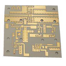
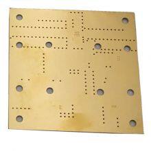
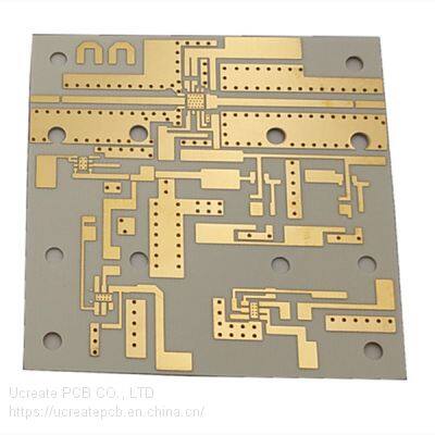
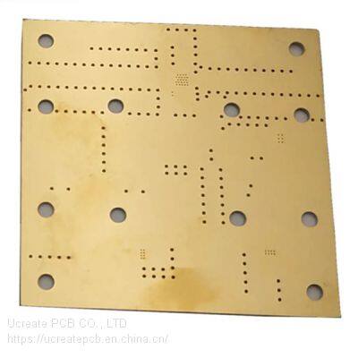
Double-Sided PCB Special Material Rogers Board
Related Products
-
 Double-Sided PCB Other New Energy PCB PCBA Board Printed Circuit Boards AssemblyUS$ 1.5 - 5.5MOQ: 1 Piece
 -
Low Cost Multilayer Rigid PCB, Multilayer Flex PCB, Rigid-Flex BoardNegotiableMOQ: 1 Piece
-
Rigid PCB / Multilayer PCB Board FabricationNegotiableMOQ: 1 Piece
-
Reliable Full Turnkey PCBA Manufacturing for Xvideo AudioNegotiableMOQ: 1 Piece
-
Ucreate PCB Assembly ServicesNegotiableMOQ: 1 Piece
Welcome to Ucreate
Ucreate is specialized in the production of a variety of single, double, high multi layers, HDI, the metallic substrate and FPC PCB. With laser drilling machine, CNC drilling machine, automatic machine, automatic exposure machine, large-scale lamination machine, Automatic flow production line, auto panel plating line, auto P.T.H Line, and other precision production equipments and AOI testing machine, flying probe tester machine and other advanced detection equipments.
We can also make quick pcb. As customers plates copied from the PCB, PCB design, prototype production, processing, and other SMT one-stop service.
Single-double sides pcb delivery time: 12-24 hours
4 layer- 8 layer pcb delivery time: 48-96 hours
Item |
Specification |
Layers |
1~32 |
Board thickness |
0.1mm-7.0mm |
Material |
FR-4,CEM-1/CEM-3,PI,High Tg,Rogers |
Max panel size |
32"×48"(800mm×1200mm) |
Min hole size |
0.075mm |
Min line width |
3mil(0.075mm) |
Surface finish |
OSP,HASL,Imm Gold/Nickel/Ag, Electric gold |
Copper thickness |
0.5-7.0OZ |
Soldermask |
Green/Yellow/Black/White/Red/Blue |
Silkscreen |
Red/Yellow/Black/White |
Min PAD |
5mil(0.13mm) |
Inter package |
Vacuum |
Outer package |
Carton |
Outline tolerance |
±0.75mm |
Hole tolerance |
PTH:±0.05 NPTH:±0.025 |
Certificate |
UL,ISO 9001,ISO14001,IATF16949 |
Special request |
Blind hole+Gold finger + BGA |
Material Suppilers |
Shengyi, KB, Nanya, ITEQ,etc. |
The double-sided PCB is a common type of printed circuit board. It has wires and components on both the front and back sides, and the double-sided PCB boards are connected with vias in the middle. The double-sided printed circuit board has two upper and lower conductor patterns, and the upper and lower via holes are connected by expensive perforations. In the processing of printed circuit boards, the hole walls of your perforated holes are coated with a copper layer to make the upper and lower layers conductive. Double-sided printed circuit boards are usually double-sided copper-clad laminates, using screen printing or photo imaging. A resist pattern is formed on the copper surface, and excess copper foil is removed by chemical etching to form a conductor pattern.
Steps to Draw Double-layer PCB Board1. Prepare the circuit schematic
2. Create a new PCB file and load it into the component package library
3. Planning the circuit board
4. Load the netlist and components
5. Automatic layout of components
6. Layout adjustment
7. Network density analysis
8. Wiring rule setting
9. Automatic wiring
10. Manually adjust the wiring
After the components of the double-layer PCB are drawn in the EDA software, the wiring sequence is first designed as power line, sensitive line, high frequency line and low frequency line. It is best to have a separate power supply for the key lead, a ground return, and the lead is very short, so sometimes a ground wire is placed close to the signal line on the edge of the key lead to make it form the smallest working loop.
The signal lines of the double-layer PCB board are the key crystal, crystal oscillator circuit, clock circuit, CPU and other signal lines, which must comply with the principle that the circulating area is as small as possible.
As one of the leading Printed Circuit Board manufacturers based in China, Ucreate has been offering international companies of all sizes with high-quality PCB prototype to production services at a fair price for eight years. To make professional and advanced circuit boards, we're committed to adhering to the strictest standards during the PCB manufacturing process. We're fully compliant with the ISO 9001:2008 quality management system.
PCB Prototype |
Quick Turn PCB |
Single-Sided PCB |
Double-Sided PCB |
Multilayer PCB |
Rigid PCB |
Flexible PCB |
Rigid-Flex PCB |
LED PCB |
Aluminum PCB |
Metal Core PCB |
Thick Copper PCB |
HDI PCB |
BGA PCB |
High TG PCB |
PCB Stencil |
Impedance Control PCB |
PCB Assembly |
High-Frequency PCB |
Bluetooth Circuit Board |
Automotive PCB |
USB Circuit Board |
Halogen-Free PCB |
Antenna PCB |
Get in Touch
Whatsapp: +8613798955467
Email: sales@ucreatepcb.com
Skype: guan418518621

Send Inquiry to This Supplier


You May Also Like
-
Oder Quick Turn PCB Prototype Assembly for Security ElectronicsNegotiableMOQ: 1 Piece
-
Medical Electronics PCB Assembly Manufacturer / 6 Layer PCBANegotiableMOQ: 1 Piece
-
PCB Assembly Services For Power ElectronicNegotiableMOQ: 1 Piece
-
Telecom Electronics PCB Assembly ChinaNegotiableMOQ: 1 Piece
-
LED Power Electronic PCBA Manufacturer ShenzhenNegotiableMOQ: 1 Piece
-
Red Soldermask Industry Control Electronics PCB AssemblyNegotiableMOQ: 1 Piece
-
Chinese Power Electric PCB Board Assembly FactoryNegotiableMOQ: 1 Piece
-
Aluminium Base PCB ManufacturingNegotiableMOQ: 1 Piece
-
Ucreate Power Bank Pcb Circuit Boards and Pcba Manufacturer SupplierUS$ 0.5 - 1.0MOQ: 1 Piece
-
Manufacturing 6 Layer HDI Printed Circuit BoardUS$ 0.5 - 1.0MOQ: 1 Piece


