

Custom ITO Glass Patterning for Experiments

Related Products
-
 ITO Coated Glass PatterningNegotiableMOQ: 1 Piece
 -
ITO Coated Glass Patterning and Selective EtchingNegotiableMOQ: 1 Piece
-
ITO Coated Glass Selective EtchingNegotiableMOQ: 1 Piece
-
Sapphire Drilling and CuttingNegotiableMOQ: 1 Piece
-
C_plane Sapphire Drilling and CuttingNegotiableMOQ: 1 Piece
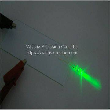
Custom designed ITO (Ag, Au or other conductive material) coated on glass or PET film
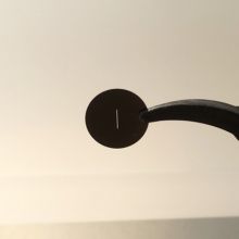
Medical sensor of Au patterning on PET substrate
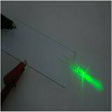
The process is developed five years ago for touch panel industry, which now is successfully replaced the wet etching process. And with long time developing and higher requirements from mobile phone industry, this process is completed and used in many other applications, mainly for developing or manufacturing sensor or circuits for OLED, medical, solar cell, consumer electronics, and many R&D cases.
We have done a lot of cases with different materials coated on different substrates, the typical one is ITO patterning, With the different absorption rates of laser, we could remove some material and no hurt to the substrate. The coating thickness usually less than 10um, and most of them is less than 1um.
The strength of this process is that it could etch 20/20um patterns which makes it possible to design the whole pattern very small and tight, and easy CAD input helps the designers have a fast prototyping and demonstration.
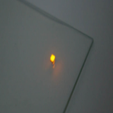
Transparant ITO glass with customized patterns
Resistance: 10~ 100 Ohm or any specially required
Transparent rate (ITO): >80%
Conductive material: ITO, CNB, CNT, nano-Ag, Graphene, and all kinds of metal coating, etc.
Min etching line width: 20um
Custom circuits area: 600*600mm
ITO single layer and double layer etching, other coating film etching, such as Ag, Al, Si removing
Precision: +/-10um
Alignment: 5um
Any patterns of CAD output
Application: touch panel, OLED, solar cell, electronics, medical, etc
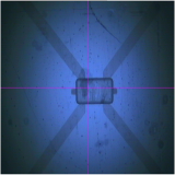
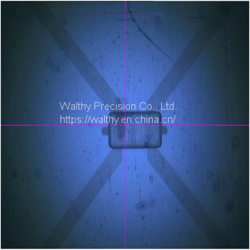
ITO patterning under microscope

Send Inquiry to This Supplier

You May Also Like
-
Optical Sapphire Drilling and CuttingNegotiableMOQ: 1 Piece
-
Optical Sapphire Wafer Drilling and CuttingNegotiableMOQ: 1 Piece
-
Optical Sapphire Subatrate Drilling and CuttingNegotiableMOQ: 1 Piece
-
Optical Sapphire WorksNegotiableMOQ: 1 Piece
-
Custom Sapphire WorksNegotiableMOQ: 1 Piece
-
Custom Sapphire WorksNegotiableMOQ: 1 Piece
-
Sapphire MicromachiningNegotiableMOQ: 1 Piece
-
Sapphire Substrate MachiningNegotiableMOQ: 1 Piece
-
Sapphire SubstrateNegotiableMOQ: 1 Piece
-
Glass/quartz/sapphire PartsUS$ 1 - 10MOQ: 1 Piece


