

Home > Electrical & Electronics > Circuit Board > PCBA > Ceramic Substrate for High Brightness LED Applications Substrate Material
Ceramic Substrate for High Brightness LED Applications Substrate Material
Negotiable
MOQ: 1 Piece (Price negotiable depending on order volume and customization)
Key Specifications
Get Latest Price
Brand Name:
Sliton
Place of Origin:
China
Model Number:
50*50
Payment & Shipping
Payment Methods:
Port of Shipment:
china
Delivery Detail:
20 days
Related Products
-
 High Power LED COB Ceramic Substrate.US$ 1 - 2MOQ: 1 Piece
 -
Spot Supply LED Ceramic Substrate, Aluminum Nitride Ceramic Circuit Board, Aluminum Nitride Ceramic.US$ 9 - 10MOQ: 1 Piece
-
Slitong Supply of LED Ceramic Circuit Boards, Factory Direct Sales Volume Favorably.US$ 9 - 10MOQ: 1 Piece
-
High Thermal Conductivity, Low Expansion Ceramic PCB.US$ 1 - 2MOQ: 1 Piece
-
Substrate Name:LED Ceramic Substrate Series.US$ 1 - 2MOQ: 1 Piece
Brand Name
Sliton
Place of Origin
China
Model Number
50*50
Surface Finishing
Silver, nickel gold, nickel palladium
Min. Line Spacing
10micron
Min. Line Width
20micron
Min. Hole Size
0.06millimeter
Board Thickness
0.25millimeter4~10millimeter
Copper Thickness
1micron~1millimeter
Base Material
Ceramic
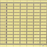
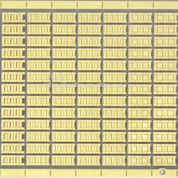
1Substrate name:Ceramic Substrate for High Brightness LED Applications Substrate material thickness:0.635mm
Conducting layer:Cu
Thickness of metal layer:75μm/75μm
Surface preparation:immersion gold
Metal single-sided / double sided:double sided
Copper plated through hole:yes
Solder mask:no

Send Inquiry to This Supplier

* Email
Want the best price?
Post an RFQ now!

Business Type
Other
Year Established
2017
Annual Export Value
US$5 Million - US$10 Million
Main Markets
North America, South America, Eastern Europe, Southeast Asia, Africa, Oceania, Mid East, Eastern Asia, Western Europe, Central America, Northern Europe, Southern Europe, South Asia, Domestic Market
You May Also Like
-
Nitride Ceramic PCB.US$ 1 - 2MOQ: 1 Piece
-
Quality Ceramic PCB For Led Lighting.US$ 1 - 2MOQ: 1 Piece
-
Alumina Ceramic PCB.US$ 1 - 2MOQ: 1 Piece
-
Double-Sided Gold-Plated Ceramic PCB.US$ 1 - 2MOQ: 1 Piece
-
Sliton Single & Double-sided Ceramic PCB.US$ 1 - 2MOQ: 1 Piece
-
COB Ceramic Substrate Integrated.US$ 1 - 2MOQ: 1 Piece
-
Ceramic Substrate for High Brightness LED Applications Substrate Material.US$ 1 - 2MOQ: 1 Piece
-
High Heat Dissipation Performance Ceramic PCB.US$ 1 - 2MOQ: 1 Piece
-
Ceramic Substrate for High Brightness LED Applications Substrate MaterialUS$ 12 - 100MOQ: 1 Piece
-
Ceramic Circuit Board Drilling Ceramic Circuit Board Cutting Ceramics Metallization-SlitonNegotiableMOQ: 1 Piece


