

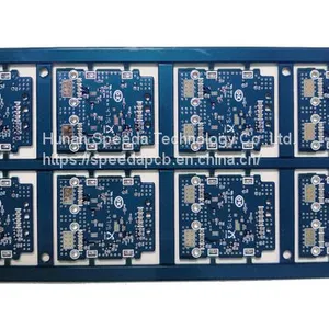
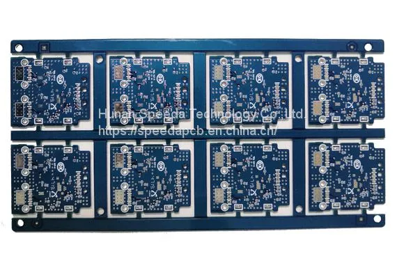
MORE PRINTED CIRCUIT LAYERS BOARD——MULTILAYER PCB
Related Products
-
 OSP PCB - PRINTED CIRCUIT BOARDUS$ 10 - 100MOQ: 1 Piece
 -
MADE OF A FLEXIBLE INSULATING SUBSTRATE——FLEXIBLE PCBNegotiableMOQ: 0 Piece
-
GOLD FINGERS PCB - GOLD PLATED PCB BOARDNegotiableMOQ: 0 Pound
-
HOT AIR SOLDER LEVELING HASL PCBNegotiableMOQ: 0 Piece
-
HDI PCB / BLIND&BURIED VIA HOLE PCB / BVH PCBNegotiableMOQ: 0 Short Ton
A multilayer printed circuit board has more layers than a double-sided printed circuit board. It has many circuit layers between the top and bottom surfaces of the printed circuit board, and each layer can be connected through PTH (plated through holes). This type is more complicated than a double-sided printed circuit board.
SPEEDAPCB, as a professional PCB supplier, is a multi circuit boards ltd. We can provide customers with a one-stop service from PCB design to PCB production and assembly.
Features of Multilayer PCB
As a professional PCB manufacturer, we have factories in Guangdong, Jiangxi, and Hunan, using advanced production equipment to ensure the high quality of our products. We have 10 PCB production lines, the machine works 24 hours a day, only to provide customers multilayer metal core pcb with satisfactory delivery time. In addition, all our products have obtained ISO-9001 quality system certification, ISO-14001 environmental system certification, and UL certification. SPEEDAPCB has been focusing on various single side PCB, double-sided PCB, and multilayers PCB manufacturing.
Multilayer pcb board simply means that more single and double boards are used to alternate the insulation material and the positioning system, and then the lines are interconnected to form a multilayer circuit board. For example, one double board is used as the inner layer and two single boards are used as the inner layer. The inner layer is a four-layer board formed by technology.
The design of the multilayer pcb fabrication is more flexible and the electrical performance is more stable and reliable. At present, the most multi-layer boards used in various industries are still four or six-layer boards, and the consumer electronics industry uses more high-level PCB boards.
Parameters of Multilayer PCB
Item |
Capabilities |
|
Number of Layers |
From 4-layer to 22- Layer |
|
Material |
FR-4, HighTg, Rogers |
|
Halogen Free | ||
PCB Thickness |
Min. thickness |
0.4mm(16mil) |
Max. thickness |
3.2mm(128mil) |
|
Surface finished |
Gold Plating |
|
Immersion Gold(Silver) | ||
HAL Lead Free | ||
Hot Air Solder Leveling(HASL) | ||
Entek Coating (OSP) | ||
Solder Mask |
Any color ,Green, White, Black, Yellow, Red, Blue |
|
Other printing |
Gold Finger |
|
Carbon Print, Peelable Mask | ||
Solder Mask Plugged Hole | ||
Copper thickness |
1/ 2 oz (18 μ m) - 4 oz (140 μ m) |
|
Min. Finished Hole Size |
0.2mm(8mil) |
|
Hole Size Tolerance (PTH) |
+/ -0.076mm (3 mil) |
|
Hole Size Tolerance (NPTH) |
+/-0.05mm (2 mil) |
|
Min. Line Width and Spacing |
0.1mm (4 mil) |
|
Min. Solder Mask Clearance |
0.05mm (2 mil) |
|
Min. Annular Ring |
0.076mm (3mil) |
|
Profile and V-Cut |
CNC-Routing, Stamping and Beveling, V-CUT, CNC |
|
Special Process |
Micro-section, Chamfer for Gold Finger |
|
File format |
Gerber ,Protel ,Autocad ,Powerpcb , Orcad ,etc |
|
TEST |
Electrical Testing , Controlled Impedance Testing , Flying Probe Test , X-Ray Inspection AOI Test |
|
Environment |
Clean room environmen , Dust-free workshop |
|
Warp & Twist |
≤ 0.7% |
|
SPEEDA Technology, founded in 2014 and located in Changsha City, Hunan Province, is a PCB design firm. We are committed to providing our customers with high-quality, high-layer board manufacturing services.

Send Inquiry to This Supplier


You May Also Like
-
High-frequency PCBNegotiableMOQ: 0 Pound
-
High Speed PCBNegotiableMOQ: 0 Short Ton
-
IMMERSION GOLD PCB / GOLD PLATING PCB / GOLD PLATED PCBNegotiableMOQ: 0 Pound
-
IMMERSION SILVER PCB - PRINTED CIRCUIT BOARDNegotiableMOQ: 0 Pound
-
Inverter AC PCBUS$ 10 - 100MOQ: 1 Piece
-
Large & Small PCBUS$ 10 - 100MOQ: 1 Piece
-
LEAD FREE HASL PCB / IMMERSION TIN PCBUS$ 10 - 100MOQ: 1 Piece
-
Medical PCB Manufacturer & AssemblyUS$ 10 - 100MOQ: 1 Piece
-
Military PCB Manufacturer & AssemblyUS$ 10 - 100MOQ: 1 Piece
-
Inverter AC PCBUS$ 1 - 100MOQ: 1 Bag

