








 Contact Platform Support
 Help Center
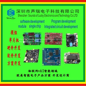
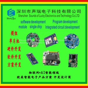
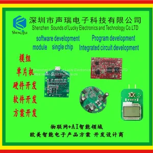
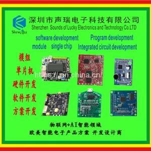
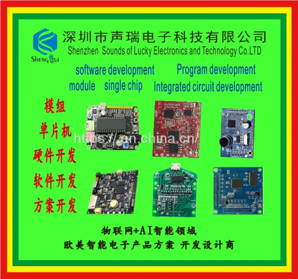
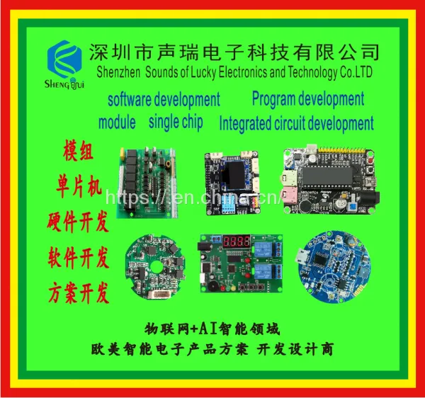
Singlechip Software Development Hardware Development
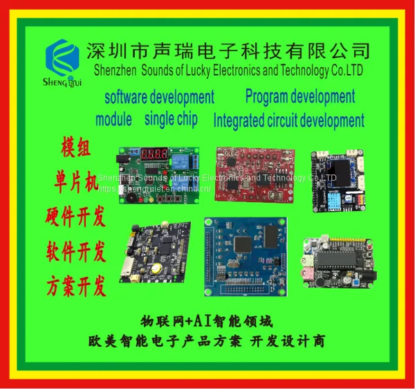
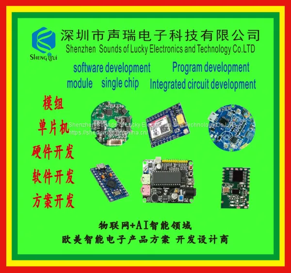
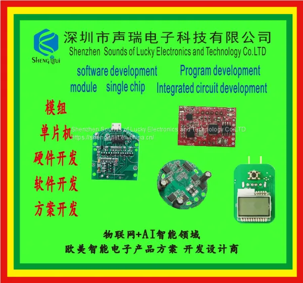



Related Products
-
 Singlechip Bluetooth Module Voice Module Hardware DevelopmentUS$ 30 - 100MOQ: 10000 Pieces
 -
Bluetooth Module Singlechip Voice Module Electronic Product DevelopmentUS$ 30 - 100MOQ: 10000 Pieces
-
Bluetooth Module Singlechip Voice Module Software DevelopmentUS$ 30 - 100MOQ: 10000 Pieces
-
Singlechip Bluetooth Module Voice Module Hardware DevelopmentUS$ 30 - 100MOQ: 10000 Pieces
-
Bluetooth Module Singlechip Development and Design of PCBAUS$ 30 - 100MOQ: 10000 Pieces
Realization of D / a conversion scheme processing by signal generator DAC chip
The application of signal generator in communication field requires not only high stability and precision, but also fast switching frequency points. The PCBA scheme of the signal generator combines the programmable gate array (FPGA) equipment with high-speed D / a chip, and uses direct digital synthesis technology (DDS) to generate continuous wave signal. DDS technology is a technology of waveform synthesis based on phase, which breaks the bondage of traditional frequency synthesis technology. Compared with traditional frequency synthesis method, DDS technology has many advantages, such as high frequency resolution, low output phase noise, continuous phase change and fast conversion speed. It is the key of all digital technology. With the development of microelectronics technology and digital integrated circuit, DDS technology has developed rapidly in recent years, It is widely used in digital communication system.
principle
FPGA is used to complete the function of DDS core, and two channels of digital waveform data are generated by parallel serial conversion technology, which is output in LVDS mode and sent to DAC chip. Finally, the analog signal with a certain frequency is output by DAC chip after digital to analog conversion.
DDS signal generating unit
The main components are a / ROM, low-pass filter and four phase accumulator. The phase accumulator and waveform storage are completed by FPGA.
At the rising edge of FPGA reference clock, the phase accumulator accumulates the frequency control words to obtain the phase to ROM addressing, completes the phase to amplitude conversion, reads out the corresponding waveform data, and outputs the stepped wave through D / a conversion.
D / a conversion
The D / a conversion sample rate is as high as 2.5gsps and RF output.
The sampling frequency of DAC chip is designed as 2gsps, and the host driver deinterleaving data is sent to these two interfaces in offset binary format. The frequency of each data channel is 1 / 2 of the chip clock frequency, that is 1GHz. Embedded DDR data clock input port (DCI), the host outputs data at the upper and lower edge of the DCI clock, and the DCI clock frequency is 500MHz. The clock edge of DCI must coincide with the data bit transition. The nominal sampling point of input data is the midpoint of DCI clock edge, which corresponds to the center of data eye. At the same time, in order to realize the synchronous operation of the host to DAC, the reference clock 4 is divided into frequency and sent to the host through the DCO interface. The frequency is the same as that of the DCI clock.
The data assembler reconstructs the two received 1GHz data streams, and reconstructs the data in the DAC core, and finally converts them into analog signals.
peripheral circuit
Refin inputs a reference frequency, which is used as the phase detector frequency after frequency division. The phase detector outputs a voltage proportional to the phase error. The external loop filter controls the noise and Spurs inside and outside the band to obtain the tuning voltage. The output frequency is the same as the set value through VCO. The output is also a differential signal, which is connected to the clock input port through a three terminal filter capacitor to provide a stable working frequency.

Send Inquiry to This Supplier


You May Also Like
-
Bluetooth Module Singlechip Program DevelopmentUS$ 30 - 100MOQ: 10000 Pieces
-
Singlechip Bluetooth Module Voice Module Hardware Development Internet of Things SensorUS$ 30 - 100MOQ: 10000 Pieces
-
Bluetooth Module Singlechip Voice Module Noise Reduction Earphone SchemeUS$ 30 - 100MOQ: 10000 Pieces
-
Singlechip Software Development Intelligent Positioning SchemeUS$ 30 - 100MOQ: 10000 Pieces
-
Bluetooth Module Singlechip Voice Modulesoftware Development Hardware DevelopmentUS$ 30 - 100MOQ: 10000 Pieces
-
Singlechip Bluetooth Module Intelligent Wearable Hardware DevelopmentUS$ 30 - 100MOQ: 10000 Pieces
-
Singlechip Internet of Things WiFi Module Wireless ModuleUS$ 30 - 100MOQ: 10000 Pieces
-
Circuit Board Program Induction Circuit Sensor ModuleUS$ 30 - 100MOQ: 10000 Pieces
-
IC,APPLE,Qualcomm,SMIC,HUAWEI,modular,Program DevelopmentNegotiableMOQ: 5000 Pieces
-
Bluetooth Module Singlechip Software Development Hardware DevelopmentUS$ 30 - 100MOQ: 10000 Pieces


