

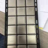
SMJ320C6701-SP Rad-Tolerant Class V, Floating Point Digital Signal Processor


Related Products
-
 ADC12J2700NKE 12-Bit, 2.7-GSPS, RF Sampling Analog-to-Digital Converter (ADC)US$ 1000 - 1050MOQ: 100 Pieces
 -
ADS54J40IRMPT Dual-Channel, 14-Bit, 1.0-GSPS Analog-to-Digital Converter (ADC)US$ 1000 - 1050MOQ: 100 Pieces
-
ADC12D1620QML-SP 12-Bit, Dual 1.6-GSPS or Single 3.2-GSPS, RF-Sampling Analog-to-Digital Converter (ADC) - AerospaceUS$ 1000 - 1050MOQ: 100 Pieces
-
AD9625BBPZ-2.5 12-Bit, 2.6 GSPS/2.5 GSPS/2.0 GSPS, 1.3 V/2.5 V Analog-to-Digital ConverterUS$ 1000 - 1050MOQ: 100 Pieces
-
AD574ASD/883 Complete 12-Bit A/D ConverterUS$ 1000 - 1050MOQ: 100 Pieces
SMJ320C6701-SP Rad-Tolerant Class V, Floating Point Digital Signal Processor
SMJ320C6701-SP Description
The SMJ320C67x DSPs are the floating-point DSP family in the SMJ320C6000 platform. The SMJ320C6701 (’C6701) device is based on the high-performance, advanced VelociTI very-long-instruction-word (VLIW) architecture developed by Texas Instruments (TI), making this DSP an excellent choice for multichannel and multifunction applications. With performance of up to 1 giga floating-point operations per second (GFLOPS) at a clock rate of 140 MHz, the ’C6701 offers cost-effective solutions to high-performance DSP programming challenges. The ’C6701 DSP possesses the operational flexibility of high-speed controllers and the numerical capability of array processors. This processor has 32 general-purpose registers of 32-bit word length and eight highly independent functional units. The eight functional units provide four floating-/fixed-point ALUs, two fixed-point ALUs, and two floating-/fixed-point multipliers. The ’C6701 can produce two multiply-accumulates (MACs) per cycle for a total of 334 million MACs per second (MMACS). The ’C6701 DSP also has application-specific hardware logic, on-chip memory, and additional on-chip peripherals.
The ’C6701 includes a large bank of on-chip memory and has a powerful and diverse set of peripherals. Program memory consists of a 64K-byte block that is user-configurable as cache or memory-mapped program space. Data memory consists of two 32K-byte blocks of RAM. The peripheral set includes two multichannel buffered serial ports (McBSPs), two general-purpose timers, a host-port interface (HPI), and a glueless external memory interface (EMIF) capable of interfacing to SDRAM or SBSRAM and asynchronous peripherals.
The ’C6701 has a complete set of development tools that includes a new C compiler, an assembly optimizer to simplify programming and scheduling, and a Windows debugger interface for visibility into source code execution.
Rad-Tolerant: 100-kRad (Si) TID
SEL Immune at 89MeV-cm2/mg LET Ions
QML-V Qualified, SMD 5962-98661
Highest-Performance Floating-Point Digital
Signal Processor (DSP) SMJ320C67017-ns Instruction Cycle Time
140-MHz Clock Rate
Eight 32-Bit Instructions/Cycle
Up to One GFLOPS Performance
Pin Compatible With ’C6201 Fixed-Point DSP
SMJ: QML Processing to MIL-PRF-38535
SM: Standard Processing
Operating Temperature Ranges
–55°C to 115°C
–55°C to 125°C
VelociTI Advanced Very Long Instruction
Word (VLIW) ’C67x CPU CoreFour ALUs (Floating and Fixed Point)
Two ALUs (Fixed Point)
Two Multipliers (Floating and Fixed Point)
Eight Highly Independent Functional Units:
Load-Store Architecture With 32
32-Bit General-Purpose RegistersInstruction Packing Reduces Code Size
All Instructions Conditional
Instruction Set Features
Hardware Support for IEEE Single-Precision
InstructionsHardware Support for IEEE Double-Precision
InstructionsByte Addressable (8-/16-/32-Bit Data)
32-Bit Address Range
8-Bit Overflow Protection
Saturation
Bit-Field Extract, Set, Clear
Bit Counting
Normalization
1M-Bit On-Chip SRAM
512K-Bit Internal Program/Cache
(16K 32-Bit Instructions)512K-Bit Dual-Access Internal Data
(64K Bytes)32-Bit External Memory Interface (EMIF)
Glueless Interface to Synchronous Memories:
SDRAM and SBSRAMGlueless Interface to Asynchronous Memories:
SRAM and EPROMFour-Channel Bootloading
Direct Memory Access (DMA) Controller
With Auxiliary Channel16-Bit Host-Port Interface (HPI)
Access to Entire Memory Map
Two Multichannel Buffered Serial Ports (McBSPs)
Direct Interface to T1/E1, MVIP, SCSA Framers
ST Bus Switching Compatible
Up to 256 Channels Each
AC97 Compatible
Serial Peripheral Interface (SPI)
Compatible (Motorola)Two 32-Bit General-Purpose Timers
Flexible Phase-Locked Loop (PLL) Clock Generator
IEEE Std 1149.1 (JTAG(1))
Boundary Scan Compatible429-Pin Ceramic Ball Grid Array (CBGA/GLP) and
Ceramic Land Grid Array (CLGA/ZMB) Package Types0.18-µm/5-Level Metal Process
CMOS Technology
3.3-V I/Os, 1.9 V Internal
Engineering Evaluation (/EM) Samples are Available(2)

Send Inquiry to This Supplier

You May Also Like
-
AD9739BBCZ 14-Bit, 2.5 GSPS, RF Digital-to-Analog ConverterUS$ 1000 - 1050MOQ: 100 Pieces
-
TLV5618AM 12-Bit, 2.5 us Dual DAC, Serial Input, Programmable Settling Time, M TemperatureUS$ 1000 - 1050MOQ: 100 Pieces
-
TL16C552AMHV Dual Asynchronous Communications Element With FIFOUS$ 1000 - 1050MOQ: 100 Pieces
-
SNJ54LVTH16245AWD 3.3-V ABT 16-Bit Bus Transceivers With 3-State OutputsUS$ 500 - 1000MOQ: 100 Pieces
-
OP200AZ/QMLV STOCKUS$ 500 - 1000MOQ: 100 Pieces
-
5962-8859301VPA STOCKUS$ 500 - 1000MOQ: 100 Pieces
-
AD6674BCPZ-1000 385 MHz BW IF Diversity ReceiverUS$ 1000 - 1050MOQ: 100 Pieces
-
XC7VX415T-1FFG1157C FPGA Virtex-7 XT Family 412160 Cells 28nm Technology 1V 1157-Pin FC-BGAUS$ 500 - 1000MOQ: 100 Pieces
-
ADS4449IZCR STOCK Quad-Channel, 14-Bit, 250-MSPS Analog-to-Digital Converter (ADC)US$ 500 - 1000MOQ: 100 Pieces
-
ADS5401IZAY 12-Bit, 800-MSPS Analog-to-Digital Converter (ADC)US$ 500 - 1000MOQ: 100 Pieces


