

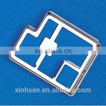
Photo Etching RF/EMI Shield Pcb

Related Products
-
 Hot Selling Stamping Shielding Case Pcb/EMI ShieldNegotiableMOQ: 100 Pieces
 -
CRS Tin WIFI PCB EMI ShieldNegotiableMOQ: 100 Pieces
-
High Precise Chemical Etched Metal ShimsNegotiableMOQ: 500 Pieces
-
Customize Phone Chemical Half Etching Copper PlateNegotiableMOQ: 500 Pieces
-
High Precision rf Shielding Metal BoxesNegotiableMOQ: 100 Pieces
Specifications
photo etching RF/EMI shield pcb1,custom design available
2,surface natural,no burrs,smooth edge
3,stable output,prompt shi
Product Description:
photo etching RF/EMI shield pcb
| Product Description | |
| Item | photo etching RF/EMI shield pcb |
| Material | Stainless steel,Aluminum,or according to customer |
| Size | custom design |
| Thickness | 0.03mm-1.5mm |
| Tolerance | +/-0.01mm |
| Certificate | Rohs,ISO9001:2008,ISO14001:2004 |
| Surface | smooth,natural,no burrs,logo added |
| Technique | chemical etching,stamping,embossing |
| Application |
many industries,Shielding Frame for electronics appliances, fixing and connecting, especially in electronic, computer, automobile, machinery, medical instrument and sport equipment |
| Finish |
Ag-plated, Au-plated, Al-plated, Cr-plated, Ni-plated, Sn-plated, Zn-plated etc(according to customer demands) |
| Structure | According to customers |
| Others | |
| Sample | Samples available within 3-6 days after payment |
| Payment | T/T,WESTERN UNION,Negotiable |
| MOQ | 100pcs |
| Packing | 25/50/100 pcs/bag,10/5/2 bags/paper case |
| Delivery | DHL,Fedex,EMS,TNT or according to customers |
E-mail: Rick(at)xinhsen(dot)com
Skype: Rick(at)xinhsen(dot)com
Product Show:
We can do all kinds of tinplate EMI Shield you want according to your requirements,just feel free to contact me for more details or send your design drawings(we will not do the same item for others,only for you)
Packing and shipping:
Packaging: 1pc/plastic bag,10 pcs/case,Or according to customer
Shipping: Within 3-6 days after payment by Air or Sea,through DHL,TNT,Fedex,EMS Or negotiable
Company Information:
Shenzhen Xinhaisen Technology Ltd.
We are a leading manufacturer handling in Chemical Etching for 8 years,still with ability to do stamping or Electroplating things.We adhere to do business on the basis of WIN-WIN and pay much attention to quality and cost control. Products:EMI/RF shield,Metal mesh,Encoder disc,VCM spacer,Metal cards,arts and crafts,logo,sign,label,some other etched things,Etc.
Sending us your drawing,We will back to you the high precision and finest products!We are always ready to be on service of you!
Company Basic Information | |
Company Name |
Shenzhen Xinhaisen Technology Ltd. |
Business Type |
Manufacturer,Trading |
Business Scope |
Chemical etching,stamping, High precision metal mesh,Encoder disc, VCM,EMI/TF shield,Filter mesh,Coffee Filter mesh,Metal Cards,Metal Crafts,Metal bookmark,logo,label,sign,tags,Etc. |
Location |
Guangdong, Shenzhen, China |
Year Established |
2012 |
Year Export |
2006 |
Employees |
100-200 |
Engineers |
10 |
Total Revenue |
US$2.5 Million-US$5 Million |
Main Market |
China mainland,America,Eastern Europe,Eastern Asia,Etc. |
Factory Area |
3000 m2 |
Certificate |
ROHS, ISO9001:2008, ISO14001:2004 |
Process Capability | |
The Min. Size |
1mm*1mm |
The Max. Size |
700mm*600mm |
Thickness |
0.03mm-1.5mm |
Thickness Tolerance |
+/-0.005mm |
The Min. Opening precision |
Φ 0.02mm |
The smallest diameter |
0.01mm |
Dimension Tolerance |
+/-0.008mm |
Elastic line tolerances |
+/-0.005mm |
The shallowest depth |
0.01mm |
Depth accuracy tolerance |
+/-0.005mm |
Special Technique |
Second on the bit,No connection point,etching and stamping |

Send Inquiry to This Supplier
You May Also Like
-
Standard Hot Sales Forge Fittings Motocycle PartsUS$ 0.5 - 5MOQ: 500 Pieces
-
AX100 THROTTLE CABLE FOR MOTORCYCLEUS$ 0.2 - 7.8MOQ: 1000 Pieces
-
China Cnc 4 Axis Machining Aluminum Spare Part MotorcycleUS$ 1 - 10MOQ: 1 Piece
-
Sigar-lighterNegotiableMOQ: 1
-
22mm ATVs Motorcycle Electric Heated Molded Silicone Hand Grips Warmers HandlebarUS$ 1 - 100MOQ: 100 Pieces
-
Motorcycle Storage Battery 12v 9ah Starter Batteries/ 12V Moto BatteriesNegotiableMOQ: 1 Piece
-
OEM Spark PlugUS$ 0.05 - 1MOQ: 10000 Pieces
-
Z250 NINJA250 Carbon Exhaust , Motorcycle Carbon Exhaust , Motorcycle Exhaust and Muffler , Motorcycle PartsNegotiableMOQ: 1 Piece
-
HGMC-L031 Aluminium Plating Motorcycle Brake LeverUS$ 0.5 - 50MOQ: 100 Pieces
-
Front and Rear Disc Brake SystemNegotiableMOQ: 1


