

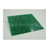
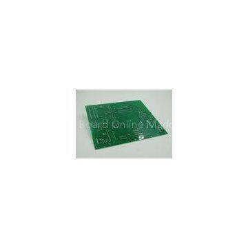
Double Layer Heavy Copper PCB 4 oz Copper Green Solder Mask HASL Finish
Related Products
-
 Lead Free HASL Heavy Copper PCB With 4oz Finished CopperNegotiableMOQ: 1 Box
 -
Gold Plating Heavy Copper PCB With Green Solder Mask / White LengendNegotiableMOQ: 1 Piece
-
6 Layer Lead Free HASL / ENIG FR4 Heavy Copper PCB High Tg and High PrecisionNegotiableMOQ: 1 Piece
-
Red Solder Mask High Current Copper Printed Circuit Board With 1 - 28 LayerNegotiableMOQ: 1 Piece
-
Variable Frequency Controller Copper Clad PCB / Rigid Bare PCB Board High DensityNegotiableMOQ: 1 Piece
Certification:UL E354810,SGS
PCB Capability
|
High precision prototype |
PCB bulk production |
||
|
Max Layers |
1-28 layers |
1-14 layers |
|
|
MIN Line width(mil) |
3mil |
4mil |
|
|
MIN Line space(mil) |
3mil |
4mil |
|
|
Min via (mechanical drilling) |
Board thickness≤1.2mm |
0.15mm |
0.2mm |
|
Board thickness≤2.5mm |
0.2mm |
0.3mm |
|
|
Board thickness>2.5mm |
Aspect Ration≤13:1 |
Aspect Ration≤13:1 |
|
|
Aspect Ration |
Aspect Ration≤13:1 |
Aspect Ration≤13:1 |
|
|
Board thickness |
MAX |
8mm |
7mm |
|
MIN |
2 layers:0.2mm;4 layers:0.35mm;6 layers:0.55mm;8 layers:0.7mm;10 layers:0.9mm |
2 layers:0.2mm;4 layers:0.4mm;6 layers:0.6mm;8layers:0.8mm |
|
|
MAX Board size |
610*1200mm |
610*1200mm |
|
|
Max copper thickness |
0.5-6oz |
0.5-6oz |
|
|
Immersion Gold/ Gold Plated Thickness |
Immersion Gold:Au,1—8u” |
||
|
Hole copper thick |
25um 1mil |
25um 1mil |
|
|
Tolerance |
Board thickness |
Board thickness≤1.0mm:0.1mm |
Board thickness≤1.0mm:0.1mm |
|
Outline Tolerance |
≤100mm:0.1mm |
≤100mm:0.13mm |
|
|
Impedance |
±10% |
±10% |
|
|
MIN Solder mask bridge |
0.08mm |
0.10mm |
|
|
Plugging Vias capability |
0.25mm--0.60mm |
0.70mm--1.00mm |
Design Guide for Heavy Copper PCB
Typical conductor width/spacing/thickness tolerance is 20%, although tighter tolerance is achievable.
The minimum width and thickness of a heavy copper PCB conductor is determined primarily on the basis of the current carrying capacity required and the maximum permissible conductor temperature rise.
A circuit board trace, depending on its size and manufacturing process, may not be rectangular in shape. Heavy copper conductors can significantly add to the overall board thickness.
Additive (plating) processed are preferred to subtractive (etching) processes but are more expensive).
Heavy Copper PCB General Info
Heavy Copper Board does not have a set of definition per IPC. According to PCB industry, however, peopel generally use this name to identify a printed circuit board with copper conductors 3 oz/ft2 - 10 oz/ft2 in inner and/or outer layers. And Extreme heavy copper PCB refers to 20 oz/ft2 to 200 oz/ft2 printed circuit board
Heavy copper normally used for a various products but not limited to: high power distribution, heat dissipation, planar transformers, power convertors, and so on
Capability of Heavy Copper PCB
Base material: FR4/Aluminum

Send Inquiry to This Supplier

You May Also Like
-
Push Button SwitchNegotiableMOQ: 2500 Pieces
-
Factory Price HAWE DG34 Hydraulic Pressure Control SwitchNegotiableMOQ: 1
-
Industrial Class Air-Conditioner Starter ACS100 Intelligence Condition SwitchUS$ 1 - 15MOQ: 5 Pieces
-
Saipwell Metal Jeans Button Custom Metal Snap ButtonUS$ 2.92 - 5.12MOQ: 100 Pieces
-
Car Fuel Tank Switch Push ButtonUS$ 2 - 6MOQ: 100 Pieces
-
Gas Range Button SwitchUS$ 0.15 - 8MOQ: 500 Pieces
-
BJ1036 Magnetic SwitchNegotiableMOQ: 1 Set
-
Singflo Waterproof Bilge Pump 3 Way Auto/off/manual Lighted Control Switch Deluxe Panel for Boat,caravan,RV.five OceansUS$ 4.5 - 5MOQ: 100 Pieces
-
Push Button Switch Remote Ip67 YL6-13 Electrical WiringUS$ 0.1 - 0.9MOQ: 100 Pieces
-
B1 Alloy Square Shape Electric Guitar Machine Head Buttons With ScrewsUS$ 0.2 - 0.5MOQ: 100 Pieces


