

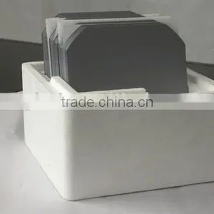
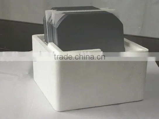
Silicon Wafer
Negotiable
MOQ: 1 set (Price negotiable depending on order volume and customization)
Payment & Shipping
Payment Methods:
Port of Shipment:
China
Delivery Detail:
Delivery time depends on order quantity.
Related Products
Place of Origin
China
| 125 Mono crystalline Wafer Specification |
| Growth Method | CZ |
| Conductive Type | P |
| Dopant | B |
| Orientation | 100 |
| Off Orientation | ±3° |
| Resistivity(ρ) | 0.5 3 Ω·cm or 3- 6 Ω·cm |
| Minority Carrier Lifetime | ≥10μs |
| Oxygen Content (Oi) | ≤1.0*1018 /cm3 |
| Carbon Content(C) | ≤5.0*1016 / cm3 |
| Dimension | 125*125±0.5mm |
| Diagonal | 150±0.5mm |
| Square Sides Angle | 90±0.5° |
| Streight Sections Length Deviation | 21.25±1mm |
| Thickness | 200±20 μm |
| TTV | ≤30μm |
| Saw Mark | ≤20μm |
| Warp | ≤75μm |
| Chips | Depth<0.3mm;Length<0.5mm |
| Appearance | No Stain, No Pinhole and Cracks by Visual Inspection |

Send Inquiry to This Supplier

Business Type
Manufacturer, Trading Company
Year Established
2001
Factory Size
30,000-50,000 square meters
Total Employees
Above 1000 People
You May Also Like
-
 2200*2200mm Solar PV Laminating Machine For Photovoltaic Solar Laminator FactoryUS$ 16,500 - 19,500MOQ: 1 Set
 -
Singflo 12v/24v dc Submersible Solar Water Pump Price for Irrgation/solar Water Pump ControllerUS$ 80 - 90MOQ: 10 Pieces
-
Solar Energy Dancing SantaUS$ 0.48 - 0.5MOQ: 500 Pieces
-
Solar Energy & UPS & Home Portable 300W Power Smart SystemNegotiableMOQ: 10 Sets
-
Solar Energy Products Solar Energy Related Products Solar Light H0228US$ 4 - 5.5MOQ: 1000 Pieces
-
Steel Solar Bracket With Black Powder CoatingUS$ 3 - 3.5MOQ: 1000 Pieces
-
Solar Panel Roof Mounting BracketUS$ 2.7 - 3.2MOQ: 500 Pieces
-
Dual-powered Battery+Solar Led Camping Solar Light for CampNegotiableMOQ: 1 Set
-
Solar Junction BoxNegotiableMOQ: 1000 Pieces
-
Protective Vents for CameraUS$ 0.1 - 3MOQ: 10 Pieces


