

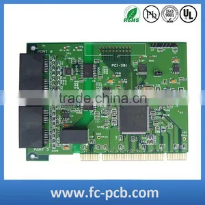
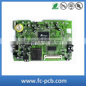
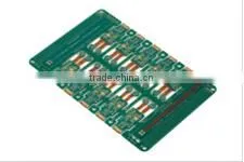
Electronics PCB Assembly/pcba Design


Related Products
-
 Pcb Board Design/Electronics PCB Assembly/cheap Rigid PcbUS$ 0.1 - 2MOQ: 5 Pieces
 -
Round FR4 Pcb Rigid Circuit Board FactoryNegotiableMOQ: 5 Pieces
-
Quick Turn Service FR4 Rigid PcbNegotiableMOQ: 5 Pieces
-
Professional Fan Double Sided Rigid PCB FactoryUS$ 0.01 - 5MOQ: 1 Piece
-
CCL Rigid PCB FabricationNegotiableMOQ: 5 Pieces
Electronics PCB Assembly/pcba design
Your Best Choice for pcb design/Electronics PCB Assembly
Quick turn for multilayer PCB design service & PCB layout
Available service :
1.PCB copy- Specializing on unlocking chip technology.
2,.PCB production service- Prototype pcb and bulk order are suiting for us.
3. PCB assembly service- Available on SMT, BGA, DIP.
4. PCB designing –Give us your specification or idea,we give u pcb what you ask.
5.Led pcb assembly- SMD different kinds of led board,suiting on Tube,Bulb,Downlight etc.
6. Electronic Component purchasing service.
TECHNICAL DATA:
Capabilities |
Standard Production |
Advanced Production |
Layer Count / Technology |
2 layer - 10 Layer |
2 layer - 12 Layer |
PCB Thickness Range |
75µm - 1600µm |
50µm - 2000µm |
Materials |
Polyimide / FR4 |
Polyimide / FR4 |
Thinnest Core |
50µm without adhesive |
25µm without adhesive |
Copper thickness |
9µm / 12µm / 18µm / 35µm |
9µm / 12µm / 18µm / 35µm |
Copper Plating Holes |
20µm (25µm) |
13µm / 20µm / 25µm |
Min. Line / Spacing |
125µm / 125µm |
65µm / 65µm ( LDI ) |
Soldermask Registration |
+/- 100µm (Photoimageable) |
+/- 50µm (Photoimageable) |
Min. Soldermask Dam |
100µm |
65µm |
Soldermask Color |
amber (green) |
amber (green) |
Cover Layer Polyimide |
laser cutting / punching / drilled |
laser cutting / punching / drilled |
Production Panel |
609,6 mm x 457,2 mm |
609,6 mm x 457,2 mm |
Min. Annular Ring |
150µm |
150µm |
smallest drill |
0,28 mm |
0,2 mm |
smalles Routing bit |
0,8 mm |
0,8 mm |
Surfaces |
OSP / Immersion Tin |
OSP/ Immersion Tin |
ID print |
White |
White |
Adhesive Tape |
Yes |
Yes |
SMT Service |
Yes |
Yes |
Stiffner material |
FR4,PI |
FR4,PI |
LEAD TIME FOR PRODUCTION ORDERS:
Sample Lead time |
Mass production lead time |
|
Single sided PCB |
1~3 |
4~7 |
Double sided PCB |
2~5 |
7~10 |
Multilayer PCB |
7~8 |
10~15 |
PCB and Assembly |
8~15 |
15~20 |
QUOTE REQUIREMENTS FOR PCB AND PCB ASSEMBLY:
- Gerber File and Bom List;
- Quantity;
- Technical requirements for quoting reference;
- Clear pictures of PCB or PCB Assembly sample if avaliable.
- Inspection method for PCB Assembly.
We make products by strict engineer processes .
We send products by vacuum package and carton box .
We always try our best! So we do,we conquer,and we get there!
Try us!

Send Inquiry to This Supplier

You May Also Like
-
Chaosheng Electronics, Ultra Long Flexible FPC, TAB Products and LED, Tape and Roll to Roll Flexible Circuit Boards, Strip Ultra Long Flexible BoardsNegotiableMOQ: 10 Blades
-
Rigid PCBNegotiableMOQ: 2600 Pieces
-
Air Conditioner Parts Pcb With Rogers Circuit Board and Gold Finger FinishedUS$ 1.56 - 2.89MOQ: 1 Piece
-
Electronic PCB Circuit Board Assembly, Electronic PCB PCBA Turnkey Service, EMS Contract ManufacturerUS$ 0.1 - 10MOQ: 1 Piece
-
Multi Layer Transparent FR-4 Circuit Board,Double Layer Transparent Circuit Board PCB,NegotiableMOQ: 1 Blade
-
PLC Controller CPM1A-8ER CPM1A-8ER FX3UC-32MT-LT CJ1W-ID231 1734-TOP 2085-OB16 2085-IF8 1746-ITB16 CQM1-OD216NegotiableMOQ: 1 Piece
-
MaAnt TY-01/02 Pro Logic Board Clamp - Clear IC ToolNegotiableMOQ: 1 Piece
-
MCPCBNegotiableMOQ: 500 Boxes
-
Custom Extra Large Thick Copper PCB BoardUS$ 0.5 - 1.0MOQ: 1 Piece
-
Printed Circuit Board(pcb) OEM AvailableNegotiableMOQ: 500 Pieces


