


Related Products
-
 SMT PCB Assembly Electronic ManufacturingUS$ 1 - 100MOQ: 1 Piece
 -
Qualified Manufacture High Quality Frequency Inverter PcbUS$ 1 - 100MOQ: 1 Piece
-
Manufacturer of Printed Circuit Board High Frequency Pcb Circuit Electronic BoardsUS$ 1 - 100MOQ: 1 Piece
-
High Quality of Bluetooth Speaker Circuit Board and Electronic BoardUS$ 1 - 100MOQ: 1 Piece
-
High Quality of Bluetooth Speaker Circuit Board and Electronic BoardUS$ 1 - 100MOQ: 1 Piece
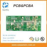
8 layer electronic assembly /electronic pcb assembly
Welcome to EASTWIN
High quality 94V0 RoHs UL power bank pcb board
We strive to provide the best contract manufacturing services
Eastwin PCB&PCBA Contract Manufacturing Services Including Blows:
v Fast PCB Fabrication for Samples and Mass Production
v Electronic Components Sourcing Services
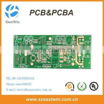
v PCBA Assembly Services:SMT,DIP,BGA...
v Function Test
v Stencil,Cable and Enclosure Assembly
v Reverse engineering service
v Standard Packing and On time Delivery
Eastwin The Most Professional OEM R&D and Electronics Assembly Contract Manufacturing Supplier In China.
*Fast Delivery:
PCB/PCBA Products 12Hours the fastest.
Provide the whole industry chain service,
From the pcb board, components purchase to pcb assembly,function testing and casing assembly.
*Engineering Support:
PCB file will be checked by our PCB engineer before production and PCBA will be test
according to our engineering testing guide.
*Customers Service:
Every feedback to our service department will be dealt with in time.
*Customers Solutions:
Provide reasonable suggestion with the pcb files design and bom list choice to Enhance the competitiveness of product in the markets.
Full Tracking:
Systematic order process, could check the production status of the entire purchase order
Main Products Application
v Household Appliances
v Medical Products
v Automotive Products
v Industrial Products
v Communication Products(AVL/GPS/GSM Devices)
v Consumer Electronics
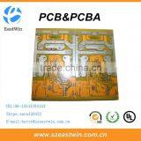
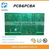
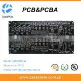
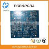
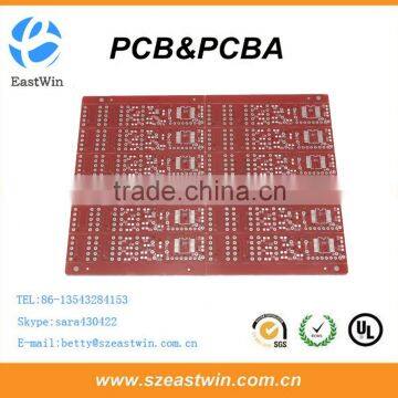
PCB Manufacturing Service
v Double-sided, Multi-layer Printed Circuit Boards
v Prototype, Pre-production and Medium to High Volume Production.
v 24 Hours Rush Delivery
v Electrical Testing
v Anti-bag packing
Testing Procedures For PCB Board
---We perform multiple strict quality assuring procedures before shipment
v Visual Inspection
v Flying probe
v Bed of nails
v Impedance control
v Solder-ability detection
v Digital metallograghic microscope
v AOI (Automated Optical Inspection)
PCB Lead Time
Layer/Days | Sample(Normal) | Sample(Fast) | Mass Production |
Single/Double | 2-3days | 24hours | 5-7days |
Four Layer | 7-10days | 3days | 7-10days |
Six Layer | 7-10days | 5days | 13-15days |
Eight Layer | 15-20days | 7days | 15-20days |
Standard Component Sourcing Service
Supplier → Components Purchase → IQC → Protection Control → Material Supply → Firmware
Technical Requirement for PCB Assembly:
v Professional Surface-mounting and Through-hole soldering Technology
v Various sizes like 1206,0805,0603,0402,0201 components SMT technology
v ICT(In Circuit Test),FCT(Functional Circuit Test) technology.
v PCB Assembly With UL,CE,FCC,Rohs Approval
v Nitrogen gas reflow soldering technology for SMT.
v High Standard SMT&Solder Assembly Line
v High density interconnected board placement technology capacity.
Quantity | Prototype&Low Volume PCB Assembly,from 1 Board to 250,is specialty,or up to 1000 |
Type of Assembly | SMT,Thru-hole |
Solder Type | Water Soluble Solder Paste,Leaded and Lead-Free |
Components | Passive Down to 0201 size BGA and VFBGA Leadless Chip Carriers/CSP Double-sided SMT Assembly Fine Pitch to 0.8mils BGA Repair and Reball Part Removal and Replacement |
Bare Board Size | Smallest:0.25*0.25 inches Largest:20*20 inches |
File Formate | Bill of Materials Gerber files Pick-N-Place file |
Types of Service | Turn-key,partial turn-key or consignment |
Component packaging | Cut Tape,Tube,Reels,Loose Parts |
Turn Time | Same day service to 15 days service |
Testing | Flying Probe Test,X-ray Inspection AOI Test |
PCB assembly process | Drilling-----Exposure-----Plating-----Etaching & Stripping-----Punching-----Electrical Testing-----SMT-----Wave Soldering-----Assembling-----ICT-----Function Testing-----Temperature & Humidity Testing |
PCB Assembly Manufacturing Procedures:
v Program Management
PCB Files → DCC → Program Organizing → Optimization → Checking
v SMT Management
PCB Loader → Screen Printer → Checking → SMD Placement → Checking → Air Reflow → Vision Inspection → AOI → Keeping
v PCBA Management
THT→Soldering Wave (Manual Welding) → Vision Inspection → ICT → Flash → FCT → Checking → Package → Shipment
Files Requested For Quote
---In order to provide you with the most efficient and accurate quote on manufacturing the requested unit, we
ask that you provide us with the following information:
v Gerber file,PCB file,Eagle file or CAD file are all acceptable
v A detailed bill of materials (BOM)
v Clear pictures of PCB or PCBA sample for us
v Quantity and delivery required
v Test method for PCBA to guarantee 100% good quality products.
v Schematics file for PCB design if need to do function test.
v A sample if available for better sourcing
v CAD files for enclosure manufacturing if required
v A complete wiring and assembly drawing showing any special assembly instructions if required
Reverse Engineering of Electronic Products
---We has developed capabilities of generating the necessary manufacturing documentation from finished
products. Services include:
v Artwork and PCB Scanning
v Schematics and Gerber File Generation
v Bill of Material and Parts List Generation
View the Details for the Gateway Controller Products we Made
View of Our Workshop
Payment Terms
Packing&Shipment Methods
Contact Us:
Sales:Betty
Tel:755-23573370-803
Skype:sara430422
Whats App:86-13543284153
Url:

Send Inquiry to This Supplier
You May Also Like
-
SG Card Ultra-thin 2-layer HDI Thick Gold Finger PCBNegotiableMOQ: 200 Blades
-
Original New A20B-8100-0661 CNC System Board Fanuc MotherboardNegotiableMOQ: 1
-
Latest Electronic Assembly GEC032US$ 0.8 - 1MOQ: 1000 Pieces
-
PCB Roger Circuit Board With Cheap Cost & Fast SupplyUS$ 0.32 - 0.56MOQ: 1 Piece
-
Customized Power Bank Pcb ,PCB Assembly Service in ShenzhenUS$ 0.1 - 100MOQ: 1 Piece
-
Enigeer Avaliable to Service Machinery 15m3 Cryogenic Liquid Nitrogen Tank for MetallurgyUS$ 28,529 - 28,610MOQ: 1 Piece
-
Electronic PCB Printed Circuit BoardUS$ 0.6 - 1MOQ: 2000 Pieces
-
Xibon Circuit BoardUS$ 9 - 10MOQ: 1 Piece
-
PCBA/PCB Assembly Service EMSNegotiableMOQ: 1
-
Home Automation Tablet LayoutUS$ 100 - 280MOQ: 1 Piece


