

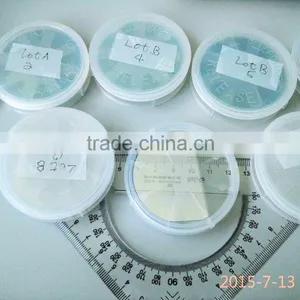
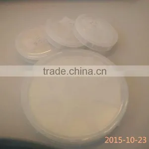
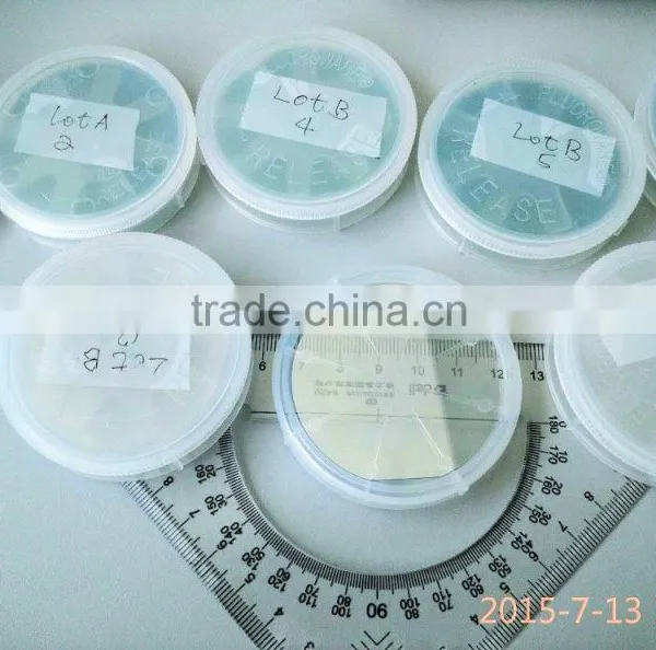
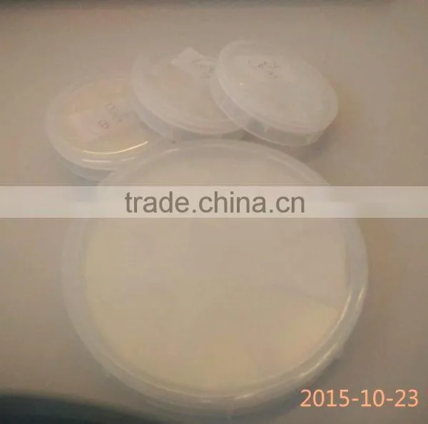
SiC Crystal Wafers for Lense and Windows
Related Products
-
 Aluminum Nitride Ceramic Substrates for High Power LD ModulesUS$ 5 - 5MOQ: 10 Pieces
 -
Carriers (Mounts) for LD/PD Stents in Optical Communication DevicesUS$ 1 - 1MOQ: 1 Piece
-
Mo/TZM BarsUS$ 50 - 50MOQ: 1 Kilogram
-
Tungsten CubeUS$ 50 - 50MOQ: 1 Kilogram
-
Tungsten BallUS$ 50 - 50MOQ: 1 Kilogram
SiC single crystal belongs to the third generation of semiconductor. It has great application prospect. As an atomic bonds compound, SiC possesses high melting temperature of 2830°C and Moh's hardness of 9.2~9.3. Compared with Si and GaAs materials, SiC has great advantages: large bandwidth, high breakdown electric field, excellent thermal conductivity, high saturated electron drift velocity. At the same time, SiC has high mechanical strength, chemical stability, strong ability to resist radiation, good thermal stability.These properties make it the preferred material in high frequency, high power, anti-irradiation semiconductor devices.
Customer customization and professional technical advisory services
Focusing on the application of new energy & new materials fields, SunEnrich Technology Co.,Ltd (SER) rely on Chinese Academy of Sciences(CAS),University of Science & Technology Beijing(USTB),China Iron & Steel Research Institute Group (CISRI),General Research Institute for Nonferrous Metals (GRINM), dedicate to the R&D and the application of rare metals (please check the pic. Of SER’s materials).
Our technical team under Doc.Zhang leadship who graduated in USTB, with ten years of work experience.
Focusing on the application of new energy & new materials fields, SunEnrich Technology Co.,Ltd (SER) rely on Chinese Academy of Sciences(CAS),University of Science & Technology Beijing(USTB),China Iron & Steel Research Institute Group (CISRI),General Research Institute for Nonferrous Metals (GRINM), dedicate to the R&D and the application of rare metals (please check the pic. Of SER’s materials). We have three manufactories located in Beijing,Shanxi Province and Guangdong Province, Beijing’s is for the R&D, Shanxi for rare materials and Guangdong is for the machining.

Send Inquiry to This Supplier

You May Also Like
-
HST-TS3 Carbon Silicon AnalyzerNegotiableMOQ: 1
-
for H8134 LENSNegotiableMOQ: 10 Pieces
-
High Quality Bk7 Plano Concave LensUS$ 2 - 49MOQ: 1 Piece
-
Infrared Laser Beam SensorNegotiableMOQ: 1 Set
-
SELON UV-6000PC UV VIS SPECTROPHOTOMETER PRICEUS$ 3,099 - 3,616MOQ: 1 Set
-
Low Price Ophthalmology Instruments China SW-2000 Ophthalmic a ScanNegotiableMOQ: 1 Set
-
Automatic Programmable Melting Point ApparatusNegotiableMOQ: 1 Unit
-
TF-C Trial Frame Sets(Color)US$ 12 - 18MOQ: 1 Piece
-
Optical Collimator,parralle Light Tube, W420-3US$ 1,400 - 1,500MOQ: 1 Unit
-
1.5M Integrating Sphere With Spectroradiometer for LedUS$ 1 - 14,000MOQ: 1 Set


